
On August 3, 2004, the MESSENGER probe1 was launched on its six-year journey to the planet Mercury. The acronym MESSENGER derives from MErcury Surface, Space ENvironment, GEochemistry and Ranging. Commissioned by NASA, and built and operated by the Johns Hopkins University Applied Physics Laboratory (JHU/APL), the probe carries a suite of scientific instruments that will conduct a study of Mercury upon entering orbit around that planet in March of 2011. Communications with the spacecraft take place through an on-board telecommunications system that includes an X-band solid-state power amplifier and three kinds of antennas:2 a high gain phased array whose main beam can be electronically steered in one plane, a medium-gain “fan-beam” antenna and a low gain horn with a broad pattern. The high gain antenna is used as transmit-only at 8.4 GHz, the medium-gain and low gain antennas transmit at 8.4 GHz and receive at 7.2 GHz, and all three antennas operate with right-hand circularly polarized (RHCP) radiation. One of each of these antennas is mounted on the front of the probe facing the sun, and one of each is mounted to the back of the probe facing away from the sun. This article describes the design and performance of one of these antennas, the medium-gain antenna.
Communication between the probe and Earth can be understood with the aid of Figure 1. Consider a spherical coordinate system whose origin is at the probe, with the z-axis pointing toward the sun. The line from sun to probe makes an angle with the line from probe to Earth; it is referred to as the sun-probe-Earth (SPE) angle and corresponds to the elevation angle ? in a spherical coordinate system. This angle can vary between 0° and 180° during the mission. Since the solar panels must always face the sun, any change to the spacecraft attitude is restricted to a roll motion about the sun-probe line; this movement corresponds to a change in azimuthal angle ?. The figure, superimposed upon the probe, shows the radiation patterns for the front and back antennas. The low gain antennas each have patterns that cover a hemisphere with maximum gains of 6 dBic. The medium-gain antennas each provide a 90° by 7.5° fan-beam with a peak gain of 15 dBic, while each high gain antenna electrically scans a 12° by 2.5° beam within a quadrant with a peak gain 28.5 dBic3 (the beamwidth specifications are for the 3 dB points). The medium- and high gain antenna patterns on the front and back of the probe sweep through a hemisphere of space as the probe is rolled about the sun-probe line. Thus the medium- and high gain antennas can provide a communication link for any location of the Earth at data rates that are medium and high, respectively, compared with the data rate of the low gain antennas.

Fig. 1 Illustration of the MESSENGER spacecraft and antenna patterns.
Electrical Design
Figure 2 is a photograph of a flight spare fan-beam antenna. It is constructed mainly of aluminum to minimize weight and to withstand the expected mission temperatures of –100° to +300°C. Various components of the antenna assembly are labeled in the figure, including an SMA-to-WR112 waveguide adapter, a diplexer, a titanium waveguide spacer and a dual E-plane waveguide bend. The radiating portions of the antenna are labeled as the transmit array and the receive array. The individual radiating elements in each array are short helix antennas. These elements are fed through the broad wall of a rectangular waveguide that is short circuited at the end. WR112 aluminum waveguide was chosen for this application because its operating band encompasses both the transmit and receive frequencies. Some electrical isolation between adjacent helices is accomplished by surrounding each helix with a short cylindrical wall. The short helix radiating elements were patterned after the design by Nakano, et al.,4 who studied the radio frequency (RF) properties of helices less than 2? long (where ? is the free space wavelength). In particular, it was shown that the short helix can produce good quality circularly polarized radiation. This property, along with a half-power beamwidth of nearly 90°, made the short helix radiator a natural choice for this application. Also described by Nakano, et al., is a linear array of short helix radiators fed by waveguide that had a matched load at one end.5 The fan-beam antenna design described here closely follows the work of Nakano, et al., with some small differences. First, the Nakano antenna is a traveling wave antenna, whereas the fan-beam antenna is a standing wave antenna. Second, the method employed to tune out the reactance of each helix probe is different. In the Nakano antenna, tuning was accomplished with capacitive stubs that are located a short distance from the helix probes. For the fan-beam antenna, tuning is accomplished with thin inductive irises that are co-located with the helix probes. A tuning element co-located with a waveguide discontinuity (the helix probe) will have interactions with the evanescent waveguide modes, and this effect must be taken into account in the design. Third, the fan-beam antenna had to withstand the temperature extremes of the space mission. This environment imposed specific requirements on helix installation techniques and compatibility of the thermal properties of materials, and necessitated thorough environmental testing. More will be said about this in the mechanical design section of the article.
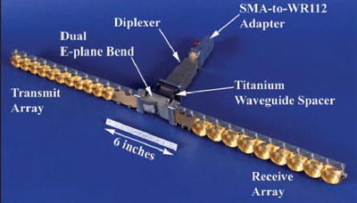
Fig. 2 The MESSENGER fan-beam antenna.
The fan-beam antenna was designed to have a minimum 3 dB beamwidth of 6° at 7.2 GHz and 5° at 8.4 GHz in the narrow cut of the pattern, and for both frequencies a minimum 3 dB beamwidth of 90° in the wide cut of the pattern and an axial ratio of 3 dB maximum. A linear array of short helices was designed for each frequency, each array having a helix separation corresponding to ?g/2 at the respective frequency (where ?g is the wavelength in the waveguide). The number of helices in each array was determined by the ?g/2 spacing and by the total array length. For the desired half-power beamwidth in the narrow cut of the pattern, the total array length L may be calculated by the approximate formula:6 L = 50°?/beamwidth. The total length is then divided by ?g/2, which yields 11 helices for the transmit array and nine helices for the receive array.
The ?g/2 helix spacing, and the short circuit located ?g/4 from the last helix, place the helix probes at the maxima of the standing wave. The electric field at adjacent maxima is 180° out of phase, and so adjacent helices are rotated about their probe axes to orient them 180° differently from each other. This arrangement allows adjacent helices to radiate in phase, even though they are being excited by an electric field that is 180° out of phase. Figure 3 shows a close-up photograph of two adjacent helix radiators; note their relative mechanical orientation is 180° apart.
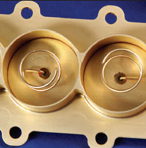
Fig. 3 The helical radiating elements.
An array, as described, can be modeled as a transmission line with N shunt admittances in parallel, where N is the number of helices in the array. This is so because of two properties of transmission lines.7 First, the value of a shunt admittance is the same when viewed from a reference plane that is n?g/2 away from the admittance (where n is an integer). Second, the short circuit at the end of the waveguide appears as an open circuit when viewed from a reference plane located (2n+1) ?g/4 from the short circuit. Therefore, a reference plane that is n?g/2 from the first helix sees N shunt admittances in parallel with each other, all in parallel with an open circuit. Transmission line theory says that the input port of the waveguide will be matched (therefore maximizing antenna radiation) when the total shunt admittance equals the characteristic admittance of the line. Since the characteristic admittance of a waveguide is a function of frequency, it is convenient to normalize it when taking measurements and therefore the goal is a total shunt admittance of unity. This means that the normalized admittance of each helix probe should be 1/N when the antenna is tuned properly.
The normalized admittance of a helix probe has a susceptance that must be tuned out. Measurements of normalized admittance were performed on one helix located ?g/4 from a waveguide short circuit, as a function of normalized probe insertion depth (normalized to the height of the waveguide). The measurement results are shown in Figure 4. As expected,8 the shunt susceptance is capacitive except for large insertion depths when the probe almost touches the floor of the waveguide. The amount of power coupled to a helix increases with larger probe insertion depth. Since the number of helices in an array was expected to be at least nine to generate the required pattern, the power coupled to each helix is modest and therefore the required insertion depth is small enough to have a capacitive susceptance. This susceptance can be canceled using a suitable inductive element co-located with a helix probe. Alternately, a capacitive tuning element located a distance ?g/4 from the probe may be used. Waveguide tuning elements have been described under the following assumptions:9 propagation of only the dominant mode, and sufficient distance from other discontinuities such that all higher order evanescent modes have decayed to insignificant levels. Interference with evanescent modes could not be avoided in the fan-beam antenna design. No matter where a matching element is placed for a helix, it will be affected by evanescent modes of that helix or modes of another helix that is close by. This outcome violates one of the above assumptions, implying that the standard formulas for a tuning element may not be accurate. It was decided to tune out the capacitive reactance of the helix probes by using a thin inductive iris co-located with each probe. Though the standard formulas for the thin inductive iris are not as accurate in this situation, the actual performance may be checked via direct measurement.
The first trial helix arrays were built by sequential tuning of the individual helices. The process began with a shorted waveguide connected to the network analyzer, and the helix closest to the short circuit (?g/4 away) was inserted through the broad wall. Heat-shrink tubing was placed on the helix probe in order to give an electrically insulating snug fit in the hole of the waveguide wall. Metal shims were inserted on each side of the probe through slits in the narrow wall of the waveguide to form an inductive iris; the slits were narrow enough to give a tight friction fit of the shims. The helix probe depth and shim insertion depth were adjusted until a normalized conductance of 1/N was obtained, with negligible susceptance. Then the next set of helix and metal shims was installed, and the combination was tuned until the total normalized admittance was 2/N with negligible susceptance. The process was repeated until all helices and inductive irises were installed, and the total normalized admittance was unity with negligible susceptance. The |S11| of the engineering model arrays was typically better than –20 dB at the center frequency.
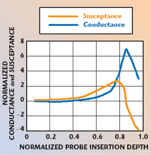
Fig. 4 Measured admittance of a helix probe versus insertion depth.
The flight helix arrays were built by parallel tuning of the helices and irises. Parallel tuning ensures that all the probes are the same and that all the inductive irises are the same. All the helices were soldered into the removable broad wall of the waveguide (described in the next section), and their probes were trimmed to a starting length. The waveguide body was machined to include inductive irises with a starting gap width. The broad wall assembly with helices was assembled to the waveguide body and a measurement of the input admittance was performed, and then the broad wall was removed again. Based on the measurement, the helix probes were trimmed and/or the inductive iris widths were machined larger. Another measurement was made, and the process was repeated until the total normalized admittance reached the center of the Smith chart. Figure 5 shows a lid assembly with helices and a waveguide body with inductive irises.
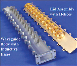
Fig. 5 The lid assembly and waveguide body for the 7.2 GHz array.
The remaining components in the fan-beam antenna assembly are as follows. The titanium waveguide spacer is meant to provide thermal insulation between the arrays, which are subject to direct solar heating, and the rest of the antenna, which is shaded by the spacecraft body. Electrically, it acts as a simple extension of the transmit and receive ports of the diplexer. The diplexer itself is a straight-junction type designed at JHU/APL and manufactured by Continental Microwave. The filter of each channel uses two appropriately spaced vanes between the centerlines of the broad walls. A cross section through the center of the broad walls is shown in Figure 6, along with measured S-parameters. A high isolation diplexer is employed elsewhere in the RF system to protect the receiver front end from the transmit power level. The SMA-to-waveguide adapter is a standard product from Continental Microwave, except that the waveguide flange was machined to a smaller height. The specified maximum operating temperature of the adapter is 120°C and is the main reason for using a titanium spacer to provide some thermal isolation between the hot fan-beam antennas and the adapter.

Fig. 6 Mechanical drawing (a) and measured performance (b) of the diplexer.
Expansion and contraction of the antenna dimensions over the temperature range from –100° to +300°C have an effect on the antenna performance. Measuring these effects on the antenna pattern while heating and cooling the antenna to these temperature extremes is very difficult and inconvenient. Fortunately, a correlation between temperature and operating frequency was established. This correlation enabled the effects of temperature to be checked by measuring the antenna performance at ambient temperature but at frequencies that are offset from the center frequency. Such measurements are shown in the Antenna Performance section of this article. To demonstrate the validity of this approach, the |S11| of the antenna versus frequency was measured at several temperatures. Figure 7 shows the |S11| of the transmit array of the antenna for three different temperatures. |S11| was measured while the array rested on a hot plate, and temperature was monitored with a thermocouple probe. The minimum |S11| at 15° and 105°C occurs at frequencies of 8.4291 and 8.4116 GHz, respectively. The temperature difference between the two traces is 90°C. Since the array is constructed mostly of aluminum, the coefficient of thermal expansion is approximately 24 ppm/°C. Multiplying this coefficient by the temperature difference gives a fraction of 0.00216, and the fractional frequency shift should correspond to (1 – 0.00216) = 0.99784. Multiplying 8.4291 GHz by 0.99784 gives 8.4109 GHz, which is only 0.7 MHz away from the frequency of minimum |S11| at 105°C, an error of only 0.008 percent.

Fig. 7 Measured return loss of the transmit array versus frequency for three temperatures.
Mechanical Design
Attaching the helices to the broad wall of the waveguide presented a challenge, because the attachment had to function electrically and also had to be mechanically robust. The final solution uses a DC feed-through structure, of the type commonly used to bring DC power through the chassis of an RF module, fastened to the helix probes. The process involves a glass-to-metal seal between the glass bead of the feed-through and the metal helix probe.10 The helices had to be fabricated of Kovar11 in order to accept the glass-to-metal seal, since Kovar has a coefficient of thermal expansion that is similar to glass. The helices with feed-throughs were then gold plated.12 The removable waveguide wall is also gold plated13 and has holes drilled to accept the feed-throughs. Helices were inserted into the holes until the feed-through flange rested on the wall surface. They were rotated about their probe axes to obtain proper phasing as described earlier, and then were soldered in place using a gold-silicon solder14 at approximately 400°C. Figure 8 shows a drawing detail of a helix with feed-through, mounted to the waveguide lid. Samples of helices soldered to the waveguide lids were put through rigorous tests to make sure that the solder bond would not fail in the flight environment. The assemblies were subjected to thermal cycling between –100° and +300°C with a ramp rate of 20°C per minute and a soak time of 15 minutes at each temperature extreme. After this procedure, the sample helices were pulled until failure of the solder bond occurred. The force required to break the solder bond was well beyond any forces the helices would experience during the mission.
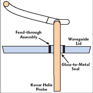
Fig. 8 Mechanical drawing of the helix with feed-through.
The flight units were subjected to six thermal cycles in a vacuum over the temperature extremes just described, with a 30-minute soak time at each plateau. Return loss was monitored before, during and after the thermal vacuum cycling, and patterns were measured afterwards to make sure that no damage was done to the antennas. The flight units were also subjected to sine vibration and random vibration along each of three orthogonal axes. The return loss was monitored before, during and after the vibration testing in order to check for damage. No damage was found on the flight units after completion of environmental testing.
Antenna Performance
Figure 9 shows plots of antenna patterns for an engineering model fan-beam antenna mounted on a flat ground plane. It shows, respectively, the wide pattern cut, narrow pattern cut and wide pattern axial ratio at three frequencies near 7.2 GHz. These patterns come close to the ideal 90° sector fan-beam shape with a reasonable axial ratio. Patterns at the transmit frequency of 8.4 GHz showed similar performance; for the flight units mounted on the spacecraft, however, the patterns were slightly distorted owing to the proximity of the high gain antenna that is tuned to the same frequency.
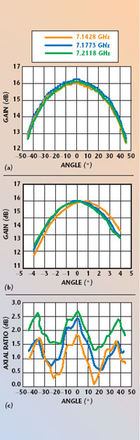
Fig. 9 Receive array patterns at 7.2 GHz; (a) wide plane, (b) narrow plane and (c) wide plane axial ratio.
The reason for measuring the patterns at three different frequencies is to gauge the effects of thermal expansion and contraction on antenna performance, as explained previously. The lower frequency extreme corresponds to thermal expansion due to a temperature increase of 200°C, while the upper frequency extreme corresponds to thermal contraction due to a temperature decrease of 200°C. The fan-beam antenna was designed for nominal performance at a temperature of +100°C, and so a ±200°C change covers the expected temperature swing of –100° to +300°C. The peak gain over this temperature swing changes by less than 0.5 dBic.
Acknowledgments
The authors wish to thank Robert Stilwell for his technical consultation and review of this manuscript. This work would not have been completed without contributions from members of the APL Mechanical Services Division, and from members of the RF Engineering Group. The MESSENGER program was sponsored by the NASA Office of Science.
References
1. A.G. Santo, et al., “The MESSENGER Mission to Mercury: Spacecraft and Mission Design,” Planetary Space Science, Vol. 49, 2001, pp. 1481–1500.
2. R.S. Bokulic, K.B. Fielhauer, R.E. Wallis, S. Cheng, M.L. Edwards, R.K. Stilwell, J.E. Penn, J.R. Bruzzi and P.M. Malouf, “MESSENGER Mission: First Electronically Steered Antenna for Deep Space Communications,” Proceeding of the IEEE Aerospace Conference, Paper 1370, CD-ROM 4-1503, Big Sky, MT, March 6–13, 2004.
3. R.K. Stilwell, R.E. Wallis and M.L. Edwards, “A Circularly Polarized, Electrically Scanned Slotted Waveguide Array Suitable for High Temperature Environments,” IEEE 2003 International Symposium on Antennas and Propagation Proceedings, Vol. 3, pp. 1030–1033.
4. H. Nakano, H. Takeda, T. Honma, H. Mimaki and J. Yamauchi, “Extremely Low Profile Helix Radiating a Circularly Polarized Wave,” IEEE Transactions on Antennas and Propagation, Vol. 39, No. 6, June 1991.
5. H. Nakano, N. Asaka and J. Yamauchi, “Short Helical Antenna Array Fed from a Waveguide,” IEEE Transactions on Antennas and Propagation, Vol. 32, No. 8, August 1984.
6. S. Silver, Ed., Microwave Antenna Theory and Design, M.I.T. Radiation Laboratory Series, Vol. 12, McGraw-Hill, New York, NY, 1948, p. 187.
7. P. Diament, Dynamic Electromagnetics, Prentice-Hall Inc., Upper Saddle River, NJ, 2000, Chapter 6.
8. N. Marcuvitz, Waveguide Handbook, M.I.T. Radiation Laboratory Series, Vol. 10, McGraw-Hill, 1948, pp. 257, 271.
9. N. Marcuvitz, Waveguide Handbook, M.I.T. Radiation Laboratory Series, Vol. 10, McGraw-Hill, 1948, Chapter 3.
10. Attachment of feed-throughs to the helices was performed by Metal Processing Co. Inc., 75 Westech Drive, Tyngsboro, MA.
11. Kovar bar stock of 0.030" diameter was obtained from Ed Fagan Inc., 769 Susquehanna Ave., Franklin Lakes, NJ; helix fabrication was done by Kirk-Habicht Co., 8905 Kelso Drive, Baltimore, MD.
12. Gold plating of helices with feed-throughs was performed by Metal Processing Co. Inc. The specification is: MIL-C-26074 Flash (Nickel Underplate) MIL-G-45204, Type 3, Class 2, 25 microinches minimum (gold).
13. Gold plating of the waveguide lid was performed at the Applied Physics Laboratory. The specification is: Zincate per ASTM-B-253, Electroless Nickel Plate 200-250 microinches thick per MIL-C-26074C, Class 1, Electrodeposit Gold Plate, 100-150 microinches thick per MIL-G-45204C, Type III, Grade A.
14. Williams Advanced Materials, 2978 Main St., Buffalo, NY, solder alloy WS363 (96.85% Au, 3.15% Si).