
An optoelectronic device performs the transition between optical and electrical components. The trans-impedance amplifier is the most suitable preamplifier configuration in optoelectronic receivers. A block diagram of the circuit module is shown in Figure 1. The trans-impedance amplifier is the first stage electrical amplifier in the receiver chain and thus enhances the input sensitivity of the receiver in the communication system. Meanwhile, the performance parameters of impedance conversion, gain, bandwidth and noise figure are very important for the trans-impedance amplifier. This optoelectronic transition is necessary to transform the optical impedance into the impedance of the microwave circuit.
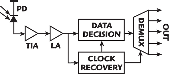
The input impedance of an optical device varies significantly in microwave circuits. Generally, the optoelectronic signals are relatively low at the input of the first stage of a receiver module, and it is necessary to increase their amplitude in the optoelectronic system. Therefore, a trans-impedance amplifier was developed. It provides gain as well as impedance transformation and converts the photocurrent into a voltage. The low noise figure and high bandwidth performance meet most of the amplifier’s specifications.
The performance of a conventional lumped element design in the trans-impedance circuit is limited by the feedback capacitance of the FET device. Hence, it is difficult to achieve a greater than 10 GHz bandwidth amplifier with a flat gain. One way to overcome this issue is to utilize a distributed amplifier, which can achieve a broad bandwidth in the gain stage of the trans-impedance amplifier. The gain-bandwidth product of the distributed amplifiers substantially exceeds the transistor unit-current gain frequency (fT) because of the input and output capacitances of the active devices. The distributed structure uses inductors to compensate for the parasitic capacitances of the devices and enhances the broad bandwidth in the trans-impedance amplifier.
This article describes the design and implementation of the microwave monolithic integrated circuit (MMIC) of the distributed trans-impedance amplifier. It uses 0.5 μm InGaP/InGaAs enhancement-mode PHEMT technology, which is appropriate for the use of a gate recess etching stop material and exhibits favorable RF characteristics.
Design of the Distributed Amplifier Circuit
In a conventional amplifier, the gain-bandwidth product is limited by paralleling the FET’s parasitic capacitance. The trans-conductance (gm) of the FET is compensated by the increase in the input and output capacitances. The distributed amplifier overcomes this difficulty by adding inductors in the circuit. The input and output capacitances of the FET can be compensated by the inductors in the distributed structures. That is, these inductors provide the circuit matching as well as compensate for the parasitic capacitances of the devices.
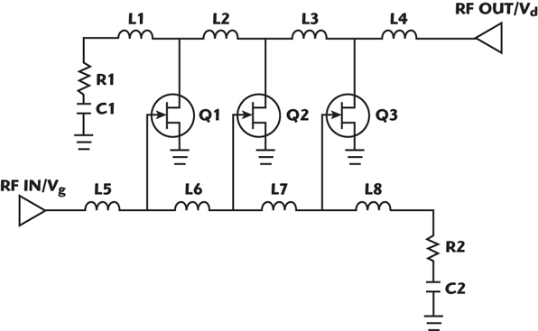
This article describes a flat trans-impedance gain and broad bandwidth distributed amplifier. In the beginning, the S-parameters, noise and trans-impedance gain of the trans-impedance amplifier were simulated by ADS (Agilent’s Advanced Design System). Considering the circuit performance and chip size, a three-stage distributed amplifier was chosen as the trans-impedance amplifier configuration. Figure 2 depicts the distributed amplifier configuration. It consists of three stages to achieve a high gain and a broad bandwidth with the input and output inductors coupled by the PHEMTs. The inductors Ll to L4 are the drain inductors, and L5 to L8 are the gate inductors. The gate and drain inductors are periodically loaded by the PHEMT gate-source capacitance and drain-source capacitance, respectively, and are terminated in the characteristic impedance at the end. As the RF signal is transmitted by the gate inductors, each transistor is excited by the traveling voltage wave and transfers the signal to the drain inductors through its trans-conductance.

The signal phase velocities on the gate and drain inductors are identical and when these signals arrive at the drain inductor output they are added in the forward direction. The out-of-phase waves, traveling in the reverse drain direction, will not be cancelled and will be absorbed by the drain-inductor’s termination. Meanwhile, the resistors R1 and R2 provide matching to the 50 Ω characteristic impedance. The capacitors C1 and C2 act as a DC block. In addition, a bias tee is used at the input port for the RFin/Vg connection and at the output port for RFout/Vg. Finally, the matching inductances and capacitances were determined and the trans-impedance amplifier was obtained, with a trans-impedance gain of 50 dB-Ω and a bandwidth of 15.2 GHz in the 2.2 to 17.4 GHz frequency range.
Device Structure and Trans-impedance Amplifier Circuit Fabrication
For PHEMT fabrication consideration, the InGaP/InGaAs E-mode PHEMT offers an excellent selective etching for the gate recess between the InGaP and GaAs, which increases the device manufacturability. In addition, the InGaP does not form DX-centers and causes less deep level defects, which results in the potential to substantially improve the reliability of the PHEMTs. Figure 3 shows the epitaxial structure of the In0.5Ga0.5P/In0.24Ga0.76As E-mode PHEMTs.
The structure includes two Si planar δ-doped layers on either side of the InGaAs undoped channel layer with an AlGaAs spacer layer for high transconductance consideration. An undoped 100 Å InGaP Schottky layer was grown on intrinsic GaAs to form a Schottky layer. Finally, two n+GaAs cap layers were grown to improve the ohmic contact resistivities. The designed structure demonstrated a sheet charge density of 2.2 x 1012 cm–2 together with a Hall mobility of 6120 cm2/V-sec at 300°K, after removing the n+ GaAs cap layer. For device fabrication, ohmic contacts of Au/Ge/Ni/Au metals were deposited by e-beam evaporation and patterned by a conventional lift-off process.
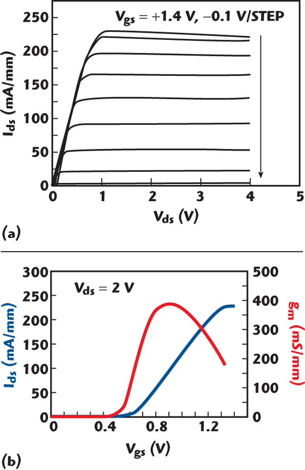
An ion-implant isolation technology was applied for mesa isolation to avoid sidewall gate leakage current. After the high selectivity succinic acid gate recess process,1 0.5 μm long Pt/Ti/Au-gates (40 Å/500 Å/4000 Å) were deposited by a lift-off process. Typical DC drain-to-source current (Ids) versus drain-to-source voltage (Vds) characteristics of the fabricated InGaP/InGaAs E-mode PHEMT are shown in Figure 4. As can be seen, the device can be operated with a gate voltage up to 1.4 V, which corresponds to a Ids of 230 mA/mm when the drain voltage is 3 V, owing to the high Schottky barrier (0.86 eV.) of the metal-InGaP contact and the large ΔEc (0.4 eV.) between the InGaP and InGaAs.2 The drain-to-source leakage current at Vds = 2 V and Vgs = 0 V is less than 0.2 μA/mm. A low drain-to-source steady-state leakage current is beneficial for suppressing the device power consumption and signal loss, particularly at low bias conditions.
The Vgs dependence of trans-conductance (gm) and Ids at Vds = 2 V are also shown. The threshold voltage (Vth) is 0.34 V (defined as Ids = 1mA/mm) and the maximum Ids and gm are 235 mA/mm and 390 mS/mm, respectively. The final circuit is achieved when the matching inductors and capacitor device are fabricated. The distributed amplifier was realized using a 0.5 μm InGaP/InGaAs E-mode PHEMT technology. A die microphotograph of the distributed amplifier, with a chip size of 0.62 mm2, is shown in Figure 5.
Measured Results
The distributed amplifier performance was measured by on-wafer probing while biased at Vgs = 0.7 V and Vds = 2.3 V, respectively. From the device Ids versus Vds characteristics, it is found that the drain current Ids is 14.46 mA when the drain voltage is 2.3 V and the total power consumption is 33.25 mW.

The S-parameters of the amplifier, including the gain, and input and output return loss, are shown Figure 6. The input return loss (S11) and output return loss (S22) remain less than –4 dB from DC to 12 GHz. Figure 7 shows the noise figure, which is lower than 5.03 dB in the frequency range from 1 to 10 GHz.
The trans-impedance gain curve, calculated from the S-parameters, is illustrated in Figure 8. The trans-impedance gain curve reveals that it is not flat. In other words, the distributed amplifier is not completely matched to 50 Ω at all frequencies, because the real part of the impedance of the gate and drain inductors remains nearly constant, whereas the imaginary part varies with frequency.

The distributed amplifier achieves a trans-impedance gain of 50 dB-Ω and a bandwidth of 15.2 GHz at the –3 dB frequency (f3dB) from 2.2 to 17.4 GHz. Table 1 lists the characteristics of recently reported trans-impedance amplifiers compared with this work. It shows that the present trans-impedance distributed amplifier has a relatively low noise figure and power consumption. Consequently, this high performance distributed amplifier, which offers a noise figure in the range from 3.34 to 5.03 dB, a DC power consumption of 33.25 mW and broadband characteristics between 2.2 GHz to 17.4 GHz, is very suitable for high speed optoelectronic transmission system applications.
Conclusion

In this article, a distributed amplifier using InGaP/InGaAs PHEMTs has been demonstrated that can increase bandwidth and reduce noise figure. The distributed amplifier was fabricated using the WIN III-V foundry 0.5 μm InGaP/InGaAs PHEMT technology. The distributed amplifier circuit consumed 33.25 mW when biased at Vgs = 0.7 V and Vds = 2.3 V, achieved a mean trans-impedance gain of 50 dB-Ω and a bandwidth of 15.2 GHz at the –3 dB frequency (f3dB) from 2.2 to 17.4 GHz. The noise figure is less than 5.03 dB in the frequency range from 1 to 10 GHz. In conclusion, the distributed amplifier has good RF characteristics and is very suitable for high-speed optoelectronic transmission applications.
Acknowledgments

The authors are grateful to WIN Semiconductors Corp. for circuit fabrication. Additional thanks are extended to the National Nano Device Laboratories, Hsin-Chu, Taiwan, for noise measurements.
References
1. H.C. Chiu, C.S. Cheng and Y.J. Shih, “High Uniformity Enhancement- and Depletion-mode InGaP/InGaAs PHEMTs Using Selective Succinic Acid Gate Recess Process,” Semiconductor Science and Technology, Vol. 21, 2006, pp. 55–59.
2. T.J. Miller, G.B. Backes and M.I. Nathan, “Schottky Barrier Height Modification on n- and p-type GaInP with Thin Interfacial Si,” Journal of Applied Physics, Vol. 76, 1994, pp. 7931–7934.
3. M. Kossel, C. Menolli, T. Mod, M. Schmalz and T. Toifl, “Wideband CMOS Trans-impedance Amplifier,” IEEE Electronics Letters, Vol. 39, No. 7, April 2003, pp. 587–588.
4. A.K. Peterson, K. Kiziloglu, T. Yoon, F. William and M.R. Sandor, “Front-end CMOS Chip for 10 Gb/s Communication,” 2002 IEEE RFIC Symposium Digest, pp. 93–96.
5. B.M.R. Samadi, I.A. Karsilayan and J. Silva-Martinez, “Design of Trans-impedance and Limiting Amplifier for 10Gb/s Optical Communication Systems,” Proceedings of the 45th IEEE Midwest Symposium on Circuits and Systems, Vol. 3, August 4–7, 2002, pp. 164–167.
6. H.H. Kim, S. Chandrasekhar, C.A. Burrus, Jr. and J. Bauman, “A Si BiCMOS Trans-impedance Amplifier for 10-Gb/s SONET Receiver,” IEEE Journal of Solid-State Circuits, Vol. 36, No. 5, May 2001, pp. 769–776.
7. R.C. Liu and H. Wang; “DC-to-15 and DC-to-30 GHz CMOS Distributed Trans-impedance Amplifiers,” 2004 Radio Frequency Integrated Circuits (RFIC) Symposium Digest, 2004, pp. 535–538.
Chia-Song Wu received his MSEE degree from Tsing Hua University, Hsinchu, and his PhD degree from National Central University, Chungli, Taiwan, in 1985 and 1998, respectively. In 1986, he joined the Chung Shan Institute of Science and Technology (CSIST), where he focused on infrared detector technology. In August 2003, he joined the department of electrical engineering at Vanung University, where he is currently involved in research on microwave and millimeter-wave integrated circuits. His research interests include OEIC and MMIC, such as laser diode, sub-micron technology, microwave, millimeter devices and MMICs.
Hsing-Chung Liu received his PhD degree in electrical engineering from Kent State University, OH, in July 1985. In 1985, he joined the Chung Shan Institute of Science and Technology (CSIST), where he focused on infrared detector technology. In March 2002, he became the dean of the R&D Office at Vanung University, where he is currently involved in research on microwave and millimeter-wave integrated circuits. His research interests include OEIC and MMIC.
Hsien-Chin Chiu received his BS and PhD degrees in electrical engineering from National Central University, Chungli, Taiwan, in 1998 and 2003, respectively. In 2003, he joined WIN Semiconductors Corp., Tao Yuan, Taiwan, where he was engaged in the research and development of 6-inch GaAs PHEMTs and related integrated circuits. In June 2004, he joined the department of electrical engineering at Chang Gung University focusing on microwave and millimeter-wave integrated circuits, fiber communication circuits and nano-technology. His research interests include deep submicron electron-beam lithography technology, solid-state physics, compound semiconductor, microwave and millimeter devices, and integrated circuits.
Wei-Hsien Lee received his BS degree in aeronautical engineering from National Formosa University, Yunlin, Taiwan, in 2003, and his MS degree in electronics engineering from Chang Gung University, Lin Kou, Taiwan, in 2006. His research interests include all areas of optical communications and millimeter-wave circuit design.