
Ku-band down-converter MMICs and receiver chips have been reported in the literature.1–3 However, for one-chip transceiver applications in Ku-band, the following problems should be solved:
• Ku-band commercial down-converter MMICs have been fabricated using GaAs MESFETs and HEMTs1–3 because they can be easily integrated on one chip with a Ku-band low noise amplifier (LNA) employing GaAs MESFET or HEMT. Owing to the high power characteristics of heterojunction bipolar transistors (HBT), power amplifiers (PA) have been fabricated using GaAs HBT in Ku- and higher frequency bands.4 However, this has been an obstacle in the realization of a one-chip transceiver solution (including PA, LNA, mixer and IF amplifier). The HBT has recently been employed for applications to an LNA, and a fairly good noise performance of 3.7 dB in the X-/Ku-bands was observed.5,6 This result indicates that, at Ku- or higher frequency bands, a down-converter MMIC, employing HBTs, is a promising candidate to realize a one-chip transceiver (including PA, LNA, mixer and IF amplifier).

• As is well known, in Ku- or higher frequency bands, an IF filter such as a surface acoustic wave (SAW) filter7 has been employed to suppress the LO leakage signal at the IF output. However, this IF filter occupies a very large area in the transceiver of a wireless communication system, which makes it impossible to integrate on a MMIC.6 Therefore, the large size of this IF filter has been an obstacle to the realization of a one-chip transceiver and has been the main cause for the comparatively high cost of transceivers in wireless communication systems.
In this article, a highly integrated down-converter MMIC, including filters, a mixer and an IF amplifier is described, which uses InGaP/GaAs HBTs5,6 for application to Ku-band one-chip transceivers. To suppress the leakage signals of the LO and its second harmonic, a spiral inductor filter, which can be integrated on MMICs due to its small size, was realized using the self-resonance characteristics of the spiral inductor. Consequently, bulky external IF filters (outside of the MMIC) were not required for the operation of the down-converter MMIC.

Integration of a Spiral Inductor Filter on a MMIC
The down-converter MMIC was designed for applications to the Direct Broadcast Satellite (DBS) system. The RF and IF frequencies are 12 and 1 GHz, respectively, with an LO frequency of 11 GHz. Figure 1 shows the circuit of the proposed down-converter MMIC. A spiral inductor, employing SiN film, was used in the filters, and the LO and its second harmonic leakage signals were suppressed to a great extent by the sharp LC resonance originating from the parasitic capacitance of the SiN film.
Figure 2 shows the top and side view of the spiral inductor structure. Figure 3 shows the equivalent circuit of the spiral inductor where the LC parallel resonance with the series resistance8 leads to the self-resonance characteristic of the spiral inductor. The spiral line is directly connected to port 1; the extended line is connected to port 2 through a contact. In order to induce a parasitic capacitance, SiN film was placed between the spiral and extended lines, resulting in a parasitic capacitance Cc occurring between the spiral and the extended lines. This parasitic capacitance plays a very important role for the self-resonance characteristic of a spiral inductor.

As shown in the equivalent circuit, Cc, Lm and Rp for the parallel resonance circuit, and the admittance Ys of the parallel resonance circuit can be expressed as

In Equation 1, Rp is much smaller than ωLm (Rp << ωLm), in the vicinity of the resonance frequency, because the metal loss Rp can be reduced by increasing the thickness of the spiral line. Therefore, Equation 1 can be expressed as

Therefore, from Equation 2, a resonance occurs at the following frequency

Equation 3 indicates that the self-resonance frequency of the spiral inductor can be controlled by Lm and Cc. The self-resonance frequency can be tuned exactly to the LO frequency by adjusting the parasitic capacitance, which makes the proposed spiral inductor structure very practical for application to LO leakage suppression. In other words, for a suppression of the LO leakage signal, the self-resonance frequency can be tuned to the LO frequency by a two-step design procedure. By adjusting Lm, the spiral inductor was designed so that the self-resonance frequency was tuned to a frequency near the LO frequency. Then, by adjusting the Cc, it was tuned exactly to the LO frequency. The inductance Lm can easily be adjusted by the number of turns of the spiral inductor. A simple equation for the inductance value Lm can be given by8

where
a = quarter of the sum of the inner and outer diameters
c = quarter of the difference between the inner and outer diameters
N = number of turns


where εSiN and dSiN are the permittivity and thickness of the SiN film, respectively, and Nc, W and T are the number of crossings between the spiral and extended lines, the width of the spiral line and the width of the extended line, respectively. Using Equations 3 to 5, the structure of the spiral inductor was optimally designed by determining the number of turns N and the width of the extended line T so that the self-resonance frequency was tuned to the LO frequency of 11 GHz.
Figure 4 shows the dependence of the self-resonance frequency on the number of turns N and the width of the extended line T for a SiN thickness of 100 nm. The calculated results were obtained from Equations 3 to 5. As shown in Equation 4, Lm is proportional to N5/3. The self-resonance frequency of Equation 3 changes substantially according to a change of N (f0 α N–5/6), which makes the tuning range of the self-resonance frequency very wide. However, fine tuning cannot be performed by only adjusting N. In this work, fine tuning of the self-resonance frequency was achieved by adjusting the capacitance Cc.
The width of the extended line T was adjusted in order to make the self-resonance frequency accurately tuned to the LO frequency (11 GHz). From Equations 3 and 5, it can be seen that the self-resonance frequency changes by a very small quantity of approximately 0.2 GHz for a 1 μm change in T, which enables fine tuning. The rate of change is 0.23 GHz/μm. The self-resonance frequency can be tuned from 11.7 to 9.4 GHz, for a range of T from 5 to 15 μm. As mentioned previously, the spiral inductor was designed by a two-step procedure to suppress the LO leakage signal. First, the number of turns N was set to six turns so that the self-resonance frequency is tuned to 10.25 GHz, which is nearest to the LO frequency of 11 GHz. Finally, the self-resonance frequency was accurately tuned to 11 GHz by selecting the appropriate value T = 8 μm. Using the above-mentioned procedure, a spiral inductor was designed to suppress the second harmonic leakage signal of the LO at 22 GHz. Accordingly, N and T were set to three turns and 7.5 μm, respectively.

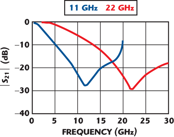
Figure 5 shows the measured insertion loss of the spiral inductors optimally designed for a rejection of the LO (11 GHz, N = 6 turns and T= 8 μm) and its second harmonic signal (22 GHz, N = 3 turns and T = 7.5 μm). As shown in this figure, the self-resonance frequency was tuned exactly to LO and its second harmonic frequency, and the spiral inductors show band-rejection characteristics in the vicinity of LO (11 GHz) and its second harmonic frequency (22 GHz). On the other hand, they show bandpass characteristics in the vicinity of the IF frequency of 1 GHz. The LO frequency rejection characteristic of the spiral inductor with N = 6 turns and T = 8 μm leads to a suppression of RF leakage signal at the IF output because the RF frequency (12 GHz) is very close to the LO frequency (11 GHz). Although the RF leakage signal at the IF output does not have a fatal effect on the performance of wireless communication systems, the suppression of the RF leakage is encouraged for stable operation of the system. For the same reason, the spiral inductor designed for a rejection of the second harmonic signal of LO (22 GHz) also highly suppresses the second harmonic signal of the RF (24 GHz).
Figure 6 is a photograph of the down-converter MMIC. The sizes of the spiral inductors for suppression of the LO and its second harmonic signals are 0.2 x 0.2 and 0.16 x 0.16 mm, respectively. Therefore, the two spiral inductors occupy a size of 0.0656 mm2 on the MMIC. The total area is only 1.9 percent of that of a conventional IF filter with a size of 2.3 x 1.5 mm2,7, which enabled the integration of the spiral inductors on a MMIC.

Performance of the Highly Integrated Down-converter MMIC Employing HBTs
Figure 7 shows the measured conversion gain. As shown, the down-converter MMIC gives only a conversion gain of 12 dB in the saturated region because it only includes the mixer and IF amplifier. Only a two-stage IF amplifier was used because the objective of this work was not to obtain a high conversion gain. Figure 8 shows the LO and its second harmonic leakage powers at the IF output at their corresponding frequencies. As shown, the leakage powers for the LO and its second harmonic signals were suppressed to a great extent by using the optimally designed spiral inductors. At a LO power of –1 dBm, the LO and its second harmonic leakage powers are –35 and –53 dBm, respectively. Considering that a LO leakage power of less than –25 dBm is required for the normal operation of commercial DBS systems including an external IF filter,1-3 the above results indicate that the down-converter MMIC, including spiral inductors, is sufficient and an external filter is not required for the normal operation of a commercial DBS system.

Conclusion
A highly integrated down-converter MMIC employing HBTs has been developed for application to a Ku-band one-chip transceiver solution. The down-converter MMIC includes a mixer, filter, amplifier and input/output matching circuits. To suppress the leakage signals of the LO and its second harmonic, spiral inductor structures employing a SiN film with a parasitic capacitance Cc were used. Considering that the spiral inductor has conventionally been used as a matching element in a much lower frequency range than the self-resonance frequency, the concept of filter application in this work is very challenging. The total size of spiral inductors for a suppression of LO and its second harmonic frequency was 1.9 percent of a conventional IF filter, which enabled the integration of a spiral inductor in a down-converter MMIC. Owing to the LC resonance characteristics of the spiral inductor structure employing SiN film, the down-converter MMIC showed a highly suppressed LO leakage power of –35 dBm and a second harmonic leakage power of –53 dBm, without an external filter, which made external filters unnecessary for normal operation of the DBS system. In addition, the LC resonance characteristics of the spiral inductors also led to a high suppression of RF and its second harmonic leakage signals. The design approach of the spiral inductor filter introduced in this article is also applicable to silicon devices as well as millimeter-wave III-V devices.
Acknowledgment
This work was supported by the Korea Research Foundation Grant (R05-2004-000-12754-0) and the second stage of Brain Korea 21. This work was also supported by the IT R&D Project funded by the Korean Ministry of Information and Communications.
References
1. E. Camargo and W. Kennan, “An E-mode GaAs FET Operating as a Single Balanced Gate Mixer,” 1996 IEEE MTT-S International Microwave Symposium Digest, pp. 951–954.
2. K. Hubbard, K. MacGowan, C. Kau, D. Smith and S. Maas, “A Family of Low Cost, High Performance HEMT MMICs for Commercial DBS Applications,” 1995 IEEE MTT-S International Microwave Symposium Digest, pp. 1649–1652.
3. Y. Yun, T. Fukuda, T. Kunihisa, T. Tanaka and O. Ishikawa, “A Low Noise and Low Power Dissipation Down-converter MMIC for DBS Applications,” Technical Journal of the IEICE, Vol. ED2001-198, January 2002, pp. 7–12.
4. M. Salib, A. Gupta, F. Ali and D. Dawson, “A 1.8 W, 6 to 18 GHz HBT MMIC Power Amplifier with 10 dB Gain and 37% Peak Power-added Efficiency,” IEEE Microwave and Guided Wave Letters, Vol. 3, September 1993, pp. 325–326.
5. K.S. Park, et al., “A Ku-band High Linearity LNA Using the InGaP/GaAs HBT MMIC Process,” Proceedings of the Asia-Pacific Microwave Conference, Seoul, South Korea, November 2003, pp. 377–380.
6. S. Kurachi, J. Chen, Y. Shimamatsu, H. Liu and T. Yoshimasu, “A Wideband Amplifier MMIC with InGaP/GaAs HBT Technology,” Proceedings of the International Symposium on Microwave and Optical Technology, Fukuoka, Japan, August 2005, pp. 764–766.
7. K. Onishi, et al., “An Application of a Flip-chip Bonding Technique to GHz Band SAW Filters for Mobile Communication,” IEICE Transactions on Electronics, Vol. E76-C, No. 6, June 1993, pp. 993–999.
8. B.C. Wadell, Transmission Line Design Handbook, Ch. 6, Artech House Inc., Norwood, MA, 1991.
 Young Yun received his BS degree in electronic engineering from Yonsei University, Seoul, South Korea, in 1993, his MS degree in electrical and electronic engineering from the Pohang University of Science and Technology, Pohang, South Korea, in 1995, and his PhD degree in electrical engineering from Osaka University, Osaka, Japan, in 1999. From 1999 to 2003, he worked as an engineer at Matsushita Electric Industrial Co. Ltd., Osaka, Japan, where he was engaged in the research and development of MMICs for wireless communications. In 2003, he joined the department of radio sciences and engineering at Korea Maritime University, Busan, Korea. He is now an assistant professor whose research interests include design and measurement for RF/microwave and millimeter-wave ICs, and design and fabrication for HEMT and HBT circuits.

In-Ho Kang received his PhD degree from Sogang University, Seoul, South Korea, in 1995. He is now a professor in the division of radio and information communication engineering at Korea Maritime University, Busan, South Korea. His research interests include LTCC and MMIC filters for the RF single chip of 5.5 GHz WLAN, WiMAX and UWB applications, including MMIC filters for power amplifier harmonics suppression.

Ji-Won Jung received his BS, MS and PhD degrees in electronics engineering from Sungkyunkwan University, Seoul, South Korea, in 1989, 1991 and 1995, respectively. From 1990 to 1992, he was with the LG Research Center. From 1995 to 1996, he was with Korea Telecom (KT). From 2001 to 2002, he was an invited researcher at the Communication Research Center, Canada. Since 1996, he has been in the department of radio science and engineering at Korea Maritime University, Busan, South Korea. His research interests include channel coding, digital modem, FPGA design technology and digital broadcasting systems.