
The past 50 years has witnessed a remarkable evolution in semiconductor technology. The devices that enable our wireless communication systems rely on sophisticated characterization. “Measuring the Q of a Parametric Diode” by Richard Harrison, the May 1960 Microwave Journal article reprinted in this month’s “Then & Now” Cover Feature series, discussed a method for parametric measurements and quantifying the value of Q of a semiconductor device almost 50 years ago. While Q continues to dictate key RF specifications from bandwidth to phase noise, the evolution of semiconductor characterization is as impressive as the advances in the devices themselves. Today’s semiconductors are measured in time and frequency domains, under small- and large-signal conditions, CW and pulsed excitations, and at measurement sweep rates that support high volume production. Device technology and test capability share a common history. In fact, the developments in test systems were made possible largely through the advances in semiconductors and vice versa. However, before any of this was possible, the microwave community relied on a powerful yet elegant duo: the S-parameter matrix and the network analyzer.
Vector network analyzers (VNA) measure the magnitude and phase characteristics of microwave devices, including passive (diplexers, couplers, filters, antennas, baluns and interconnects, for example) and active components (power amplifiers, LNAs, mixers and switches, for example) as well as multi-functional MMICs/RFICs. These test systems operate by comparing the incident signal supplied by the analyzer with either the signal transmitted through or reflected from the device terminals. With phase measurements come scattering, or S-parameters, which are a shorthand method for identifying these forward and reverse transmission and reflection characteristics. Phase data also adds vector error information, which permits error correction of the measurement system and minimizes measurement uncertainty. Phase measurements also allow for measuring group delay, which is the “rate of change of phase vs. frequency.” Throughout many years of service, S-parameters and the network analyzer have provided microwave engineers with invaluable device information, transcending the role of test equipment and data to become vital components in the design process. This article looks back at the 50-year evolution and current state of the test equipment responsible for measuring S-parameters.
The Early Days of Microwave Device Characterization
At low frequencies, voltages and currents (and impedance) are used to represent the electrical properties of an electrical circuit at a certain instant in time. When the excitation frequency increases to the point where the physical size of the circuit has the same order of magnitude as the associated wavelength, wave propagation must be taken into account. Voltage and current can no longer be defined unambiguously. For this reason, microwave engineers are forced to replace voltages and currents with incident and reflected waves as a means to characterize devices. In 1965, an IEEE article entitled “Power Waves and the Scattering Matrix” by Kaneyuki Kurokawa of Bell Labs was among the first technical papers to popularize the concept of the scattering matrix, today referred to as S-parameters. This form put transmission, reflection and impedance into a single two-dimensional representation, which could be readily measured and easily visualized, thus revolutionizing high frequency measurement and design (see Figure 1).
In the 1960s, the emergence of reflection, transmission and S-parameter measurements were critical to the engineers beginning to design with newly available high frequency semiconductors. These early microwave measurements were performed using test systems implemented with rudimentary signal generators, power detectors and impedance bridges. A similar system based on a signal generator, slotted line, standing wave meter and lossless variable transformer was described in the aforementioned “Measuring the Q of a Parametric Diode” article.
The standing wave detector or SWR meter (HP415E) used to measure diode Q in Harrison’s 1960 article was actually an AC voltmeter with a narrow filter centered at 1.000 kHz. Many of the signal generators from that period had a built-in 1 kHz modulation to support the use of the “VSWR meter”. Prior to the network analyzer, the procedure described in this article was fairly common. The method was both tedious and time-consuming. Hand-tuned measurements were taken one frequency point at a time using a swept scalar analyzer combined with painstaking, point-by-point reconstruction of the relative phase characteristics of devices. It was not uncommon to spend an entire day measuring enough data in order to construct a Smith chart with a reasonable band of frequencies. Before the network analyzer, microwave measurements also suffered from inadequate error-correction. Transistor measurements were especially problematic because they required either an open or short termination on the transistor often causing the device to break into oscillation.
The Birth of the Network Analyzer
Even back then, advances in semiconductor and measurement technology went hand-in-hand. For instance, samplers based on semiconductor diodes became the fundamental building blocks of instrumentation. These were used to sample waveforms and measure the signal’s relative amplitude and phase. Agile signal sources based on backward-wave oscillators allowed measurements to be taken across a wide frequency range. Based on a vector voltmeter, the first network analyzer capable of swept amplitude and phase measurements was the HP8407 RF network analyzer from Hewlett-Packard (predecessor to Agilent Technologies). This early network analyzer allowed comparison of the amplitude and phase of two waveforms, but it operated only up to 110 MHz.
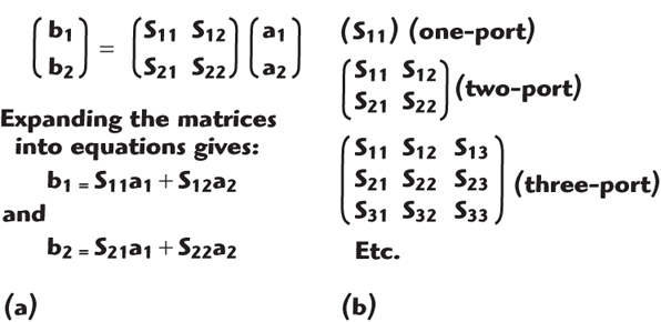
In 1967, Hewlett-Packard (HP) introduced the model HP8410 network analyzer (see Figure 2). This system extended swept frequency capability up to 12 GHz and revolutionized S-parameter measurements at microwave frequencies. The HP8410 could display data directly on a CRT screen, which allowed engineers to view the device response in real time and even permitted the tuning of a device under test. This bench-top system was composed of several instruments performing various functions integrated into a single unit. The source module or signal generator provided the stimulus to the device under test (DUT). The test set module routed the stimulus signal to the DUT and sampled the reflected and transmitted signals. The frequency range of the source and test set modules established the frequency range of the system. Frequency conversion occurred in the analyzer. The analyzer module down-converted, received, and interpreted the IF signal for phase and magnitude data. It then displayed the results.
The two main modules of the HP8410 RF section included a sampler, used to convert the RF signals into lower frequency signals suitable for digital signal processing, and a synthesizer to provide the necessary excitation to the device under test. The RF heart of the HP8410 system was the HP8411A “Harmonic Converter.” Instead of using a sampling pulse generator, the samplers were driven by a harmonic generator (via a SRD driven by a VCO). The harmonic converter relied on a variable frequency oscillator to generate harmonics way up into the microwave region and act as the local oscillator to the reference and test mixers which in turn provided signal to the reference and test input ports. The down converted intermediate frequency was fed back into the HP8410 main frame. A socket on the front or rear panel of the network analyzer test set was available for adding a longer reference line to balance the phase (an important consideration for measuring phase linearity) associated with the electrical length of the DUT and the connecting coaxial test cable.
Octave band sweep oscillators using a backward wave oscillator (BWO) plug-in module drove the early test sets. The plug-in included a plastic ruler that snapped over the frequency pointers to give the user a rough idea of the frequency. A wave meter in series with the setup was often required to accurately know the frequency. A combiner box held the three plug-ins and a controller allowed sweeping across a frequency range covered by the three BWO modules. Solid-state sweepers would eventually be capable of sweeping greater frequency ranges.
Early Displays
Unlike the sophisticated display technology of today, early data displays were rather crude and relied on various dedicated CRT hardware plug-ins. For instance, the Phase Magnitude Display was the display of choice for looking at gain or loss vs. frequency in real time. Grease pencils were often used to temporarily record a response during tuning or to indicate the pass/fail specification during production testing. The polar display CRT was useful for impedance measurements and matching. Smith chart overlays of different magnifications were available to translate trace position into impedance values. The Phase Gain Indicator meter was another popular display, allowing users to expand the meter scales for more resolution during manual measurements.
Computers: Disruptive Technology—1970s Style
S-parameters and the network analyzer led to more bench-top tuning and improved design efficiency via build and test prototyping. As the network analyzer became a design tool, greater accuracy (error-correction) and increased data collection was needed. By the late 1970s and early 1980s, computers (especially the PC) were often used to expand instrument capabilities. Computer-controlled network analyzers such as the HP8542 introduced error correction mathematics, pulsed measurements, “large-scale” production testing and other capabilities to this test system. Many engineering groups developed their own computer-controlled systems based on need and desire to improve the software and/or calibration methods.
Due to the electrical characteristics of the cables and fixturing that supplies the signal to the DUT, there will be electrical delays and losses between the reference and test signals that are not contributed by the DUT. These effects must be calibrated out of the measurement before any accurate data can be retrieved. For phase vs. frequency measurements, early network analyzers used an extended coax reference line to equalize the signal with the length of the test arm. Software and computer-controlled network analyzers, however, provided a far superior approach to handling the path length differences and system losses.
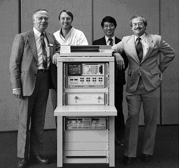
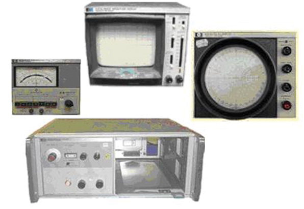
Despite the improved accuracy and automation made possible by computer control, these early systems were large, containing up to three racks of equipment. Eventually, network analyzers would realize all of this capability in a single bench-top box including a synthesized source, receivers, test set and display thanks to solid-state sources, improved samplers and microprocessors. Network analyzers of the mid-1980s (see Figure 3) fueled the microwave component development and manufacturing that coincided with the high-levels of avionics and radar activity taking place during the Reagan administration. The first fully error-corrected RF network analyzer offering lower cost and higher capability came to market just as the manufacturing demands for the first generation of cell phones was growing (see Figure 4). Meanwhile the RF semiconductor technology that was made possible by the network analyzer was also being used to build the next generation of test equipment.
Addressing the Wireless Market
The early 1990s ushered in the wireless device boom and the first high frequency consumer market. Communication devices and their components (RFICs/MMICs, discrete and hybrid modules) would not only need to support complex performance brought on by digital modulation techniques, they would also be subject to cost pressures and high volume manufacturing. Many mobile communications systems would use time-domain duplexing leading to the need for pulsed measurements. Many devices also included frequency conversion devices, as well as balanced inputs or outputs. Such devices required more than two excitation ports. Frequency conversion devices such as mixers required a network analyzer with a frequency-offset mode to allow the source stimulus and the response receivers in the analyzer to be independently tuned to different frequencies. All of these challenges had to be met without giving up fast measurement throughput and dynamic range. The network analyzer would evolve once again to meet these challenges.
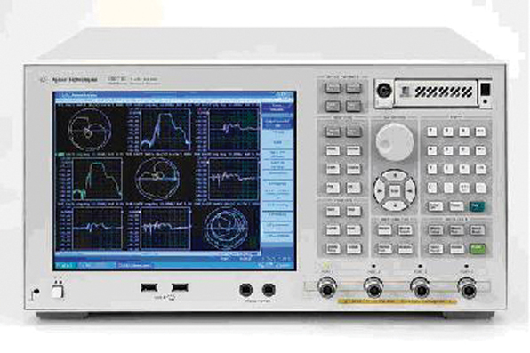
By the late 1990s the nature of commercial RF components changed in several significant ways. Circuits started using balanced (differential) topologies in order to take advantage of lower power requirements and higher isolation. A key improvement for testing these devices came in 2001 with the introduction of Agilent’s ENA (E5071A), the first four-port network analyzer designed for the mass production market (see Figure 5). In addition to differential I/Os, new and highly integrated devices at both the chip and package level resulted in a large number of input/output (I/O) ports. Measuring the performance of individual IC elements, particularly with respect to isolation became a challenge. As the number of required measurements grew by N-squared (N represents the numbers of ports), characterizing higher port devices with existing VNAs became impractical.
Differential I/Os and Multi-port Devices
The next generation of test sets to be introduced extended the port count of the network analyzer even further. These N-port systems use internal switches and couplers to seamlessly integrate the test set with the analyzer giving the N-port test set a level of performance that is directly comparable to that of two- or four-port systems. There are eight- and 12-port versions of N-port network analyzers currently available, with 16- and 32-port systems soon to follow.
All major VNA manufacturers (Agilent, Anritsu, Rohde & Schwarz) today offer multi-port systems for characterizing devices such as diplexers, circulators, directional couplers, differential transmission lines and active components such as mixers. Calibrating a multi-port instrument can be time-consuming if done conventionally. Therefore, techniques have been developed to greatly shorten the calibration process, including the use of electronic calibration modules, which provide a full NxN matrix of calibrated measurements with only N-connection steps.
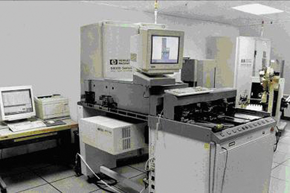
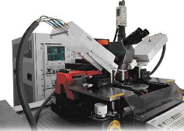
Auto-calibration modules provide fast, repeatable and high quality coaxial calibrations. Test port cable converter kits also allow a single module to calibrate insertable and non-insertable devices. However, most semiconductor measurements today are performed while the devices are still in wafer form. The development of the wafer probe from Cascade Microtech was instrumental in allowing VNA measurements to be performed at the chip level, eliminating the need to place a device in a package and test fixture. RF wafer probes allow the excitation and measurement of closely located device ports. Combined with the automated probe station, today’s chip testing is quite sophisticated, supporting research and development as well as high-volume production testing (see Figure 6).
Combining the Network Analyzer with Other Measurement Systems
RF semiconductor devices must work over a wider range of operating conditions than 50 years ago. To keep pace with the device requirements, test systems are integrating more functionality, supporting multiple tests such as large-signal S-parameters, power and spectral measurements for CW and pulsed operations all with a single device connection. Because the network analyzer also corrects for mismatches between the DUT and test equipment, combining it with more complex stimulus-response test systems offers more accurate results. Network measurement systems can now also address large-signal and pulsed operations. In 2007, Rohde & Schwarz introduced the first measurement system to combine a full-featured vector network analyzer with a spectrum analyzer in a single portable instrument that can perform both reflection and spectral measurements such as adjacent-channel power or third-order intercept, as well as measurement of UMTS, WLAN, or WiMAX signals. The optional spectrum analysis capability also supports phase noise, noise figure and high-accuracy power measurements.
Large-signal Measurements
Transistors used in RF and microwave applications must be characterized dynamically (large-signal operation) in order to determine compression characteristics, inter-modulation and spectral re-growth. A nonlinear network measurement system is a stimulus/response system, similar to a vector network analyzer but used to characterize the large-signal device behavior completely under a periodic stimulus (see Figure 7).
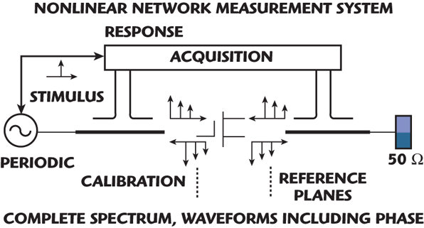
The system includes a test set to separate incident and reflected waves. A microwave source injects a signal into the DUT. If this component is nonlinear, it will generate harmonics. These harmonics are reflected back by the mismatch created by the measurement system. A broadband acquisition system is able to take proper samples of the broadband incident and reflected waves. The systematic errors of the measurement system are eliminated using proper calibration techniques. The complete spectrum (amplitude and phase) of incident and reflected waves can be acquired and the time waveforms reconstructed.
These same network measurement systems can also be used to determine power performance while accounting for test system/DUT impedance mismatches. Many VNAs have built-in capabilities for analyzing specific device performance metrics. For example, the Anritsu 37000D VNA provides an automated power flatness calibration program for characterizing test port power. By providing flat output power from the analyzer test port over the frequency range, this system allows optimum swept frequency gain compression measurements. When calibrated with the Anritsu ML24XX series power meters, the calibration routine automatically stores a power correction table in the analyzer for later recall. The result is a vector network analyzer with high power at the test port and power meter accuracy. Capabilities such as this use to be the realm of custom built systems and software developed in-house.
Balanced Large-signal Measurements
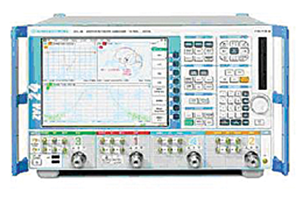
Options available for the R&S ZVA and ZVT analyzers with three or more ports introduced “true” differential VNA measurements, providing accurate results for balanced active devices operating under large-signal conditions. The option also allows two signals to be generated, with 0° or 180° of phase shift, to produce true common-mode or differential mode measurements with a conventional single-ended VNA. The phase shift does not vary with time and temperature variations, a significant breakthrough in itself, since it is one of the primary reasons why this technique could not be achieved previously. The sources are controlled with a special algorithm and control circuitry that precisely maintains the magnitude/phase relationship. Traditionally, balanced devices measured in the nonlinear large-signal region almost invariably overstated device performance. As a result, manufacturers would specify their products inaccurately.
Using the true differential technique, gain compression may occur at lower drive levels than when measured using the conventional technique. The result is that amplifiers will produce unacceptable levels of intermodulation products under conditions that were previously thought to meet specifications. Testing with differential inputs under large-signal conditions allows manufacturers to specify their parts conservatively ensuring they will meet their rated performance under actual operating conditions. This nonlinear region is of vital interest to the device designers employing the orthogonal frequency division multiplex (OFDM) modulation technique, such as WiMAX, lightwave communications and cable systems in order to ensure extraordinarily high levels of linearity. In addition, when the Long Term Evolution (LTE) enhancement to UMTS wireless systems is deployed in a few years, it too will require the same level of linearity.
Pulsed Measurements
In many mobile communications systems and radar applications, devices must often be characterized with a pulsed RF signal or a pulsed control voltage. With pulsed stimulus signals, S-parameters can be measured at the correct drive without exceeding destructive power or temperature levels. By using an appropriate duty cycle, the average power can be reduced significantly while maintaining a high peak power. In addition, many components for radar systems only exhibit their desired performance and effectiveness under pulsed stimulus conditions. The VNA measures the effect that the DUT has on the pulsed stimulus. Since the VNA performs ratio measurements, any non-ideal behavior of the pulses themselves is removed from the measurement.

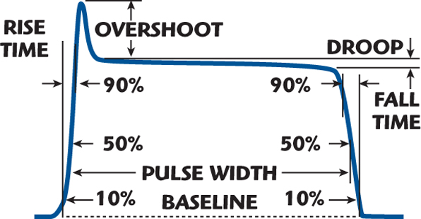
The point-in-pulse measurement enables accurate S-parameter and power measurements by shifting the moment of data acquisition within the pulse. This technique eliminates the dependency of dynamic range on duty cycle; however, it does require a VNA with a wide measurement bandwidth. Using the point-in-pulse measurement technique, the pulse is monitored only during the “on” phase of the RF bursts so the sampling time (Tspl) to acquire the raw data of a wave quantity or an S-parameter must be shorter than the pulse width, ton (see Figure 8).
By selecting a suitable trigger delay, the start of the sampling process can be shifted by the designer to the point of interest such as the quiet “pulse roof” of the active device. Dynamic range and sensitivity using the point-in-pulse method depends on sensitivity and the measurement bandwidth of the receivers, which are independent of the duty cycle of the RF pulse. Consequently, dynamic range depends on pulse width, which limits sampling time and thus the required measurement bandwidth. Averaging can be applied to increase dynamic range by maintaining the measurement bandwidth.
To analyze the time-dependent behavior of a device during a burst, the VNA must perform a so-called “pulse profile” measurement (see Figure 9). The pulse profile method can be performed with most VNAs in conjunction with an external setup for pulse profile measurements. Disadvantages include the inability to analyze non-periodic pulses, double pulses, pulse trains, or complex modulated pulsed signals. The technique requires recalibration with a change of duty cycle, suffers from low dynamic range for low duty cycles and requires high resolution, which results in low measurement speed.
Rohde & Schwarz employs wideband detection and fast data recording to improve pulse profile measurements (see Figure 10). Pulse profile analysis or S-parameter measurements with pulsed stimulus is limited by the sampling rate of the A/D converter, the processing time between two consecutive data points and the available bandwidth. Sampling rate and data processing time between two data points limit the time resolution, while the measurement bandwidth determines the minimum rise and fall time of the pulse that can be analyzed. Options for select VNAs reduce bottlenecks by uncoupling the data acquisition process from the data processing step in order to make pulse profile measurements with high resolution at high speed. The R&S approach is to sample the raw data and store it directly without filtering, allowing the instrument firmware to immediately perform the digital down-conversion and filtering. An A/D converter continuously samples and digitizes the data at 80 MHz and writes it into high-speed RAM. The technique produces fast yet detailed and accurate pulsed profiling. It combines fast throughput (more than 10 sweeps/s over 1001 test points) with time pulse resolution of 12.5 ns/point.
The PNA-X Series of VNAs from Agilent Technologies can supply either a CW or pulsed stimulus and accurately measure the CW or pulsed responses. The pulse-measurement timing is generated by an integrated pulse generator, which has four main output channels, each with independent delay and width. The output channels can be routed internally inside the PNA-X to drive the modulators and acquisition circuitry, and/or externally to drive external peripheral devices. Since these pulse generators are independent of the measurement channels, each measurement channel can have independent pulse generator setting. This allows the simultaneous measurement and display of a variety of measurements, including pulse-profiling, point-in-pulse and gain compression on a single display.
The PNA-X VNA can make pulse measurements in wideband and narrowband modes. The two modes have benefits and trade-offs. Modern VNAs such as the PNA-X include both detection modes so that operators have the flexibility to tailor their measurements to the characteristics of the DUT. Wideband detection is suitable for cases when the majority of the pulsed RF spectrum falls within the bandwidth of the VNA’s receiver.
The advantage of the wideband mode is that there is no loss in dynamic range for low-duty-cycle pulses, with a relatively constant signal-to-noise ratio (SNR) versus duty cycle. The disadvantage is that there is a lower limit on measurable pulse widths. As a signal’s pulse width becomes narrower, the spectral energy is spread over a wider bandwidth. When enough of the pulse’s energy falls outside of the receiver’s bandwidth, the receiver can no longer properly detect the pulse.
In narrowband detection mode, the pulse width is usually much less than the minimum time required to digitize and acquire one discrete data point. With this technique, the entire pulse spectrum is removed by filtering except the central frequency component, which represents the frequency of the RF carrier. After filtering, the pulsed RF signal appears as a sinusoid or CW signal. With narrowband detection, analyzer samples are not synchronized with the incoming pulses (therefore no synchronized measurement trigger is required), so the technique is also known as asynchronous acquisition mode. This approach is also called the “high PRF” mode because the PRF is usually high compared to the receiver’s IF bandwidth.
Current Network Analyzers
What capabilities do today’s network analyzers offer? Speedy measurements are paramount to collecting the vast amount of S-parameter data needed to represent high frequency semiconductors operating in the current generation of wireless devices. The latest VNAs offer impressive capabilities in the following areas:
• Performance—includes wide dynamic range, fast measurement speed (time for frequency sweep, switching times between channels and setups), high output power, wide power sweep range and accuracy
• Multi-port capability—includes two, four or more ports with direct access to all generator and receiver paths
• Versatility—includes advanced network measurement capabilities such as large-signal analyses, frequency converters, balanced circuit topologies, pulsed, intermodulation, hot S-parameters and integrated spectrum analysis
• Usability—powerful yet user-friendly interface for measurement control, custom automation and data visualization (post-processing functionality)
• Connectivity—and data acquisition via high speed data exchange (GPIB, USB and WLAN)
• Portability—vendors are now offering small, light, portable vector network analyzers suitable for field applications (calbe loss, distance-to-fault, system frequency response, etc.)
Conclusion
For nearly 50 years, S-parameters and the network analyzer have been a fundamental source for characterizing component behavior. This measurement system made the evolution of the RF/microwave semiconductor possible to the extent that measurements played a critical role in component design. In turn, the VNA benefited directly from using the technology that it was responsible for measuring. This bootstrapping, which began 50 years ago, continues today. Wherever the need for stimulus/response characterization exists, the network analyzer will be there, measuring the attributes of new devices and materials, adapting to address the needs of new applications, operating conditions and parametric analyses.
Feedback:
David
Enjoyed the article on Network Analyzers. I would like to provide some added information on two of the figures.
The individuals in Figure 3 are two UofW faculty members and two HP employees. http://www.ee.washington.edu/about/centennial/looking_back/index.html
At the UofW web site the UoW professors are identified as Prof. Daniel and Prof. Yasuo Kuga. And the HP folks are on the far right is Bill Wurst, General Manager (in 1985) of Network Measurement Division (NMD) of HP and the second person on the left was Scott Wright, then Marketing Manager of NMD (Later a general manager at HP and later at Anristu).
Figure 4 is an HP84000 which was a good ten years (probably 1994 or so to 2001) after the HP8510 introduction. The 84000 was a new architecture of analyzers (not a re-use of an existing architecture / hardware) and was capable of absolute power, NF, spectrum analysis and inter-mods in addition to network analysis - and had an frequency range of 8 GHz plus. It was capable of 2 to 8 or more ports. It was targeted at automated RFIC chip testing in a high volume manufacturing environment.
The use of the figure and the text it is in embedded in does not quite match. The article text is "The first fully error-corrected RF network analyzer offering lower cost and higher capability came to market just as the manufacturing demands for the first generation of cell phones was growing (see Figure 4). Meanwhile the RF semiconductor technology that was made possible by the network analyzer was also being used to build the next generation of test equipment."
The comment of "first fully error-corrected RF network analyzer" does not really fit the 84000 -- other products existed years earlier (8510, 8753, 8720, ... and non-HP products) and the 84000 was a more complete measurement system than a standard network analyzers.
Great article
John Barr, Agilent EEsof RFIC Product Marketing
For readers interested in keeping up with the latest advances in network analyzer technology, the manufacturers have excellent reading material on the current state of technology and measurement techniques. Some interesting material is listed below:
Agilent
Application Note 1408-12: Pulsed-RF S-parameter Measurements Using Wideband and Narrowband Detection
http://cp.literature.agilent.com/litweb/pdf/5989-4839EN.pdf
Article reprint 5989-6353EN:
http://cp.literature.agilent.com/litweb/pdf/5989-6353EN.pdf
Anritsu
Application Note No. 11410-00387: Primer on Vector Network Analysis
www.us.anritsu.com/downloads/files/11410-00387.pdf
Application Note No. 11410-00383: Power Measurements—Handheld Site Master™/VNA Master™/Spectrum Master™/BTS Master™/Cell Master™ Products
www.us.anritsu.com/downloads/files/11410-00383.pdf
Application Note No. 11410-00300: Pulsed S-parameter Measurements
www.us.anritsu.com/downloads/files/11410-00300.pdf
Application Note No. 11410-00329: S-parameter Measurements with Multiport Balanced Test Sets
www.us.anritsu.com/downloads/files/11410-00329.pdf
Application Note No. 11410-00197: Measuring Frequency Conversion Devices
www.us.anritsu.com/downloads/files/11410-00197.pdf
Rohde & Schwarz
Application Note 1MA124_0E: Tackling the Challenges of Pulsed Signal Measurements
www.rohde-schwarz.com/appnote/1MA124.html
Application Note 1EF48: Power Measurement on Pulsed Signals with Spectrum Analyzers
www.rohde-schwarz.com/appnote/1EF48.html
Application Note 1EZ52: Antenna Measurements, RCS Measurements and Measurements on Pulsed Signals with Vector Network Analyzers R&S ZVM, R&S ZVK
www.rohde-schwarz.com/appnote/1EZ52.html
Application Note 1MA32: Noise Figure Measurements on Amplifiers in Pulsed Mode
www.rohde-schwarz.com/appnote/1MA32.html
Additional VNA Information Featured in March at www.mwjournal.com
Expert Advice
Dr. Joel Dunsmore, senior R&D engineer/scientist with Agilent Technologies, discusses the enhancements and trade-offs that enable VNAs to move beyond S-parameters, and the improvements in these measurements brought about by extending the calibration capabilities of VNAs into other measurement classes.
Read & reply to this month's Expert Advice
Retrospective
Michael Hiebel, from Rohde & Schwarz and author of Fundamentals of Vector Network Analysis, gives a European perspective of the development of VNAs from the days of the slotted line, to the present day and beyond as he identifies potential future developments.
Read this month's Retrospective