
 In today’s environment, the Band-Reject Filter (BRF), or Band-Stop, is the solution of choice in an increasing number of cases. Exhibiting low loss and good power-handling, this device offers high attenuation of unwanted signals in a localized area, while impacting the entire remaining spectrum very little. Where communication systems are bundled together in close proximity, as is often the case in the commercial wireless domain and in the battlefield scenario, the BRF is considered the appropriate solution for interference mitigation.
In this article, we follow a natural extension of this trend to the next component level, in the form of the Band-Pass / Band-Stop (BP-BS) Diplexer, to show how new real applications are supported. BP-BS Diplexers span a wide range of specifications, ranging from two doubly-terminated filters to singly-terminated cases connected together, leaving the designer to simulate parallel connections and minimize mutual interactions using optimization routines.
While the Band-Pass Filter (BPF) has received a great deal of coverage in the literature, the BRF has received relatively little, often forcing the design engineer to rely on intuition and imagination. The need for fast and accurate responses to customer requirements mandates that a new design strategy be devised.
What is a BP-BS Diplexer?
A BP-BS Diplexer is a three-port device that allows three frequency bands to be combined or divided through the common port; the middle passband travels through the BPF, while the lower and upper passbands travel through the BRF. Each filter can exhibit All-Pole (AP) or Quasi- Elliptic (QE) response, also known as Pseudo-Elliptic response. In the AP case, the order of the filter is the number of poles at DC or Infinity. A QE response is described by a Transfer Function consisting of Poles at DC or Infinity and Zeros at prescribed frequencies. (The word "Quasi" arises from cases in which transmission zeros are not part of the inverters, as they are with true Elliptic response.) Filters are realized in the technology of choice that supports the required un-loaded Q of the individual resonators. These technologies include Lumped Elements (coils and capacitors), Distributed Elements, such as TEM, Micro-Strip, Strip-line, Suspended-Substrate and Strip-Line, and Wave-Guide structures, to name a few. In the search for the right combination, the engineer starts by calculating the transfer function for each filter, i.e., the number of poles and zeros, and then takes into account parameters such as operational frequency, un-loaded Q, power-handling, size, higher-order modes, etc.
Each aspect of the design (at least for the BPF case) is well covered in existing literature, and the details are outside the scope of this article. In general, MYJ [1] presents a BP-BS Diplexer using direct synthesis of the elliptic BPF, and Snyder [2] and Cameron, et al., [3] provide good information about Quasi-Elliptic BRF.
The Design Strategy
As mentioned earlier, optimization routines play an important role in minimizing the mutual interactions between filters and shaping final response. This author believes that in the case of QE response BRF with skewed slopes (asymmetric), no direct synthesis has yet to be reported. In summary, here are the requirement steps defining our design strategy:
1) Quick estimation of Transfer Functions for both filters.
2) Creating a net list of the BP-BS Diplexer.
3) Carry out an optimization to refine the final response.
4) Translate the net list into the technologies of choice to realize the diplexer.
5) Obtaining crucial information such as location of zeros, mutual couplings, etc., from the optimized net list to aid in the tuning process.
6) Use 2.5D and 3D simulators to verify broadband response and ensure first-pass yield in production.
In many cases, stages 1 and 2 are covered by in-house programs; however, there are commercially available software packages such as PCFILT, S/FILSYN, ComNav’s Dionysus, and others that can handle the task. While stage 3 is supported by linear simulators, including past and present offerings from Agilent EEsof EDA (GENESYS, legacy Touchstone, etc.), stage 4 is entirely in the engineer’s hands. At this point, many other important factors come into play, such as cost, material lead-time, etc.
Assuming that QE Low-Pass Prototype (LPP) networks are used, we begin the examination of stage 5 by looking at the mutual coupling formula between two resonators as given in [1], and we encounter the first serious problem:
I.  Where giand gi+1are the g-values of the LPP network and W is the fractional bandwidth of the BPF.
Since the net list is already optimized, calculating with g-values means that we need to convert the networks back to normalized Low-Pass Filter (LPF) to check how the g-values changed, an impossible task given the time constraints. Further, if we used a direct synthesis procedure, then the solution to the approximation problem was never based on g-values. Thus, a new set of equations needs to be developed taking the generalized form of equation (I), unless the Transfer Functions of the filters are to be presented in terms of N+2 by N+2 matrices. (The matrix option makes it possible to obtain all the information needed. This method is extremely accurate and purely mathematical, not building or relying on engineering intuition. More information about this choice can be found in [4].)
Stage 6 is known to be very time consuming, but it can pay dividends if the project goes into production. Software products such as Sonnet and HFSS, to name a few, can provide crucial information, such as accurate aperture sizes and gaps for minimal tuning, as well as power-handling and re-entries that affect ultimate rejections. Reducing the time for stage 6 is possible if stages 1 through 5 are properly addressed.
The BPF Structure
Using [2], we represent the BPF by lumped elements as shown in Figures 1 and 2. These expressions take into account all possible RF paths typically used to create transmission zeros in both the Real (Delay) and Imaginary (Amplitude) domains. The resistors associated with the un-loaded Q of the resonators have been removed for simplicity, but are taken into account during the simulation. This model provides accurate results for the coupling values, but fails to predict re-entries, hybrid modes, and self-resonances, consequently failing to predict ultimate rejections, as well. For a certain degree of confidence, the AP distributed model and referral to previous measurements of similar designs are helpful. Otherwise, the only true predictor of out-of-band spurious response is stage 6 analysis.

Figure 1 - General Coupling Formulas for the Inductive Case

Figure 2 - General Coupling Formulas for the Capacitive Case
The BRF Structure
Using [3], we start by representing the BRF by a set of parallel connected open stubs (OS) separated by odd multiples of _-wavelengths for the AP case, or non-commensurate lines that differ from _-waves for the QE case, as shown in Figure 3.
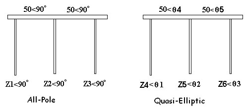
Figure 3 - Direct Coupled All-Pole and Quasi-Elliptic BRF
The coupling coefficient of each resonator to the main line is given by:
II. 
Where:
Ζ1 = Impedance of Shunt Resonator
Ζ0 = Impedance of Main Transmission Line
ƒ0 = Center Frequency in MHz
KBW is the expression for "Loading Bandwidth" in MHz and is measured by the distance between the -3dB points around the resonant frequency.
Since the self -impedances of the OS resonators get higher as percentage bandwidth decreases, some (or all) of these impedances can’t be realized. In response, the shorted-stub capacitive-coupled model is used as an alternative, as shown in Figure 4. Self-impedance is set and shunt capacitors to ground are added, mainly so that all resonators have the same length. Figure 5 shows the analysis of a shorted-stub capacitive-coupled resonator.

Figure 4 - Shorted-Stub Capacitive-Coupled Resonator Model

Figure 5 - Analysis of the Shorted-Stub Capacitive-Coupled Resonator

Figure 6 - Reflection, Delay, and Coupling
The Generalized BP-BS Diplexer
The network depicted in Figure 7 represents the BP-BS Diplexer in its most general form. Additional shunt capacitors connected at the ends of each BSF inverter are to improve the matching of the upper passband. By replacing a _-wavelength (or close to _-wavelength) segment with a three-section LPF, it is possible to increase the upper effective passband, described in [3]. Please note that the suggested input loading of the BPF is a series capacitor. In this case, the BRF will be able to pass DC signals without interruption. On the other hand, the BPF output can take any form, including tapping, transformer or series capacitor. The BPF might have any form of QE response by having several RF-paths. In this example, a series capacitor bridges over an even number of resonators, which results in having a pair of transmission zeros, one below and one above the passband. Using the equations given earlier, the engineer can obtain all necessary design data from the optimized net list.

Figure 7 - BP-BS Diplexer General Form
BP-BS Applications
The following are three types of applications for which the BP-BS Diplexer could be the solution of choice:
Mixers and Up/Down Converters
Spurious outputs return to the mixer and cause additional beats. Consider placing a BP-BS Diplexer instead of a pad attenuator and BPF. Although the idea is not new, this alternative has only recently begun to gain in popularity, perhaps because of past difficulties associated with BRF design. At low frequencies, amplification is cheap, but at higher frequencies, the pad attenuator (3dB to 6dB) and BPF option involves expensive gain and increased noise. Figure 8 compares the two approaches, and Figures 9 through 12 show an X-band example.

Figure 8 - Suggested Use of BP-BS Diplexer in Mixers and Up/Down Converters

Figure 9 - X-band BP-BS Diplexer Information

Figure 10 - BRF Filter in X-band BP-BS Diplexer

Figure 11 - X-band BP-BS Diplexer

Figure 12 - X-band BP-BS Diplexer Measured Response
Broad-Band Measurement of Output Emission
In this suggested application, we measure the output emission of electronic appliances operating at full power. This requires terminating the carriers and passing the IM products unaffectedly. Strong attenuation of main carriers, on the order of 90dB, is needed to prevent those signals from entering the spectrum analyzer / power meter, etc.

Figure 13 - High-Power BP-BS Diplexer

Figure 14 - Typical Response of High-Power BP-BS Diplexer with QE Response
Combining Two Transmitters (a Third Base Station) to a Common Antenna
It often occurs in the field of wireless communication that a service provider with two bands of interest desires to share a common antenna with a second provider with a single band, without causing interruptions. In this case, the BP-BS Diplexer must handle high CW and peak powers, requiring special attention in the design stage.

Figure 15 - Using a BP-BS Diplexer to Add a Second Transmitter and Third Base Station
Conclusions
Improved QE BRF design methods make the BP-BS Diplexer the solution of choice for certain new applications. Advances in the purity of materials yield improved components, such as better capacitors, permitting designs that can meet more stringent requirements, such as increased power-handling and reduced space. This article seeks to make system engineers aware of advantageous new application possibilities and to assist component engineers in supporting related demands.
References
1) G. Matthei, L. Young, and E. M. T. Jones, "Microwave Filters, Impedance-Matching Networks, and Coupling Structures."
2) Kawthar Zaki, Ralph Levy, and Rafi Hershtig, "Synthesis and Design of Cascaded Trisection (CT) Dielectric Resonator Filters."
3) Richard V. Snyder, "Quasi-Elliptic Compact High Power Notch Filters Using a Mixed Lumped and Distributed Circuit," IEEE Transactions on Microwave Theory and Techniques, Vol. 47 No. 4, April 1999.
4) Richard J. Cameron, Chandra M. Kudsia, and Raafat R. Mansour, "Microwave Filters for Communication Systems."