
The technical definition of an amplification class is not obvious. Patents are among the best documents to explain and define what an amplification class is.1,2 Reviewing the claims sections of those documents is an interesting exercise in understanding the inherent complexity of an amplification class definition.
From a simplified point of view, an amplification class can be defined by a set of electric conditions that must be fulfilled simultaneously at the output of a transistor. Usually, these electric conditions are a set of current and voltage waveforms in the time domain or their counterpart set of load impedances/admittances at fundamental and harmonic frequencies, obtained as the quotient of the Fourier series voltage and current components. A proper load, with simultaneous proper driving, leads transistors towards any specific amplification class. This definition of amplification class, based on spectral load-pull analysis, is especially useful at high frequencies because many of the design techniques used at these frequencies, measurement procedures, etc., rely on the power of spectral analysis.
Table 1 shows the load impedance or admittance required by a single-ended ideal transistor at the fundamental and harmonic frequencies when operating in the most popular amplification classes. The load impedances and admittances shown were obtained as the quotient of the Fourier components of a transistor’s output voltage and current waveforms. The transistor is considered ideal and lossless (pure current source or switches).
Broadband RF High efficiency Power Amplifier Design
The following few steps describe a straightforward way to design broadband power amplifiers, high efficiency or not, based on load synthesis theory:
• From the desired output power POUT and power supply DC voltage VDC, determine the load impedance or admittance required by the transistor operating into the selected amplification class. The values given in the table help to predict the load’s frequency profile. The maximum transistor’s values of voltage and current impose a limit for power supply DC voltage and output power POUT.
• Design a network to provide the load calculated in step 1 over the whole desired bandwidth. The required load must be provided both at the fundamental and harmonic frequencies, at least the second and third.3
• Provide the proper driving waveform (energy in time) required by the transistor to exercise the output voltage and current waveforms inherent of the desired amplification class. High efficiency amplification classes usually require transistor switching and therefore these classes, such as classes D or E, demand more sophisticated driving circuits than conventional classes (A to C) because more energy must be delivered to the transistor input (gate or base) in a shorter time.
The next few sections will explain how to design broadband power amplifiers operating in some of the most popular RF amplification classes: B, C, D and E, although the described design strategy can be applied to any amplification class.

Broadband Class-B Power Amplifier
The admittance required by classes B and C is resistive at the fundamental frequency and short circuits at the harmonics. These load conditions (compatible with class-A) can be easily accomplished when using RF transistors, because their output capacitance COUT can be embedded into the output load network contributing to the generation of the required short-circuit condition at harmonics.
Usually, communication electronics textbooks4 have used parallel tuned R-L-C tank circuits across the transistor output to illustrate class-B and -C circuits. When those circuits are tuned at the fundamental frequency amplified by the circuit and their quality factors are high, they provide the required load conditions for class-B and -C operation, generating typical class-B and class-C voltage and current waveforms if the transistors are properly driven. Unfortunately, the high quality factor required for the parallel load networks (needed to achieve a sufficient strong short-circuit condition at the second and third harmonics) contribute to narrow the amplifiers’ bandwidth.

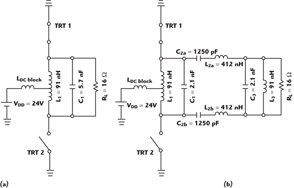
Figure 1 shows class-B (or -C) amplifiers using classical R-L-C circuits shown in textbooks. Figure 2 shows the simulated output powers POUT and drain efficiencies ηd of the class-B amplifiers. This load network has a loaded quality factor Q = 4 at 7 MHz. All the circuit elements are considered ideal, linear and lossless.
A broadband class-B amplifier design requires a load circuit providing the same admittance profile provided by the narrowband version, but obviously over a wider bandwidth. One of the circuits capable of providing such load admittance is a bandpass filter with a shunt first element. If a strong attenuation at the stop band is provided, a strong short-circuit condition at the harmonics is provided also. The bandpass of the filter must coincide with the desired amplification band while the suppressed band must coincide with its harmonics. This circuit is shown in the figure. Usually filter orders higher than three (six lumped elements) are not suitable for RF and MW amplifiers because the element losses and finite Q reduce the efficiency of the amplifier. This fact limits the design flexibility and broadband performance forcing the designer to accept some tradeoffs, including ripple in the bandwidth or amplification class purity, for example. The broadband load network shown is intended for a class-B (or -C) amplifier designed on the basis of a Chebishev bandpass filter, blending a wide bandwidth, low ripple over its bandpass and strong suppression of harmonics (which means low impedance at harmonics). All the circuit elements are ideal and lossless. A remarkable power and efficiency bandwidth improvement over the narrowband circuit is observed.
The uniform harmonic requirement of classes B and C (short circuit) is quite compatible with the loading effect of the transistor’s intrinsic output capacitance COUT. Therefore, broadband operation of class-B amplifiers is not uncommon and there are examples of class-B push-pull designs in literature exhibiting multi-octave bandwidths.5 Amplifiers intended for 50 Ω systems usually require impedance transforming networks to provide the required resistive load to the amplifier. In broadband design, broadband impedance transforming networks are required also; these transforming networks must be capable of transforming at least one or two harmonics besides the fundamental. There are two usual solutions for this problem:
• Using broadband transformers usually based on transmission lines.
• Using broadband impedance transforming networks based on lumped elements or transmission lines.
These impedance-transforming networks can also be used to include the loading functions described in the broadband RF high efficiency power amplifier design section. Unfortunately, the bandwidth of a network combining transforming and loading functions is smaller than the bandwidth of a load network without transforming duties for the same number of elements.
High Efficiency Broadband Amplifiers
Among high efficiency amplification classes, those based on transistor switching, such as classes D and E, are known for their extremely high efficiency, theoretically 100 percent. Their popularity in the RF and MW world is increasing, but still some misunderstanding about these amplification classes exist; for instance, some engineers still think that narrowband is a requisite of high efficiency amplification. Nevertheless, high efficiency wideband switching amplification design is possible using the techniques shown previously.
Class-D
Two versions of the class-D amplifier6 are widely known: current switching and voltage switching (voltage switching class-D is sometimes confused with class-F).
As shown in the table, a transistor requires alternate harmonic load behaviour to operate into class-D: open circuits at (2n+1)f0, short circuits at (2n)f0 for voltage switching class-D, short circuits at (2n+1)f0 and open circuits at (2n)f0 harmonics for switching current class-D. This nonuniform harmonic load cannot be provided easily to a transistor operating at high frequencies for different reasons. The low reactance exhibited by the transistor’s intrinsic output capacitance COUT is one of them. The load requirements of class-D make it difficult to absorb COUT into the amplifier load network, especially in the switching voltage mode. This is one of the causes that contribute to preclude class-D at high frequencies.
The alternate frequency dependance nature of the load impedance required for class-D cannot be easily provided by a single-ended wideband load network design, even though some solutions exist. Unlike single-ended transistors, push-pull transistor pairs require uniform load impedance distribution over frequency from drain to drain (drain-to-source load requirements are the same as for the single-ended version) to operate into class-D and this is the reason why class-D amplifiers are usually shown as push-pull designs in classical textbooks.4 The most usual textbook load circuits capable of providing switching current class-D amplification are shown in Figure 3.
The operation of a nominal switching current class-D requires a quality factor Q approximately greater than four for the parallel tank L1-C1-R1 of the load network, in order to provide proper termination at the harmonics. Unfortunately, high values of Q also contribute to reduce the bandwidth of the amplifier. Decreasing Q is not a solution to improve amplification bandwidth because low Q leads to amplification class degeneration caused by improper loading at harmonics.
It is possible to design broadband switching class-D amplifiers using the design techniques shown previously. The application of the described technique is quite easy for push-pull designs using ideal transistors (COUT = 0) because a uniform load at the harmonics is required from drain to drain. Unfortunately, the intrinsic transistor capacitance COUT located across the real transistor’s drain and source tends to lower the impedance load at the harmonics, degrading the open-circuit condition required by voltage switching class-D at (2n+1)f0 harmonics and current switching class-D at (2n)f0. However, current switching class-D is a better candidate for high frequency broadband operation than the switching voltage version of class-D, because the COUT effect over mode degradation is less evident.

A bandpass filter with a shunt capacitor as a first element can provide the load conditions required by an ideal push-pull transistor pair to operate into wideband current switching class-D, because the load impedance profile requirements of the pair are the same as the conditions required to operate into class-B (the driving requirements are completely different). The load circuit shown for broadband has been designed this way using a third-order Chebishev bandpass filter (ripple=0.01 dB). Figure 4 shows the output power Pout and drain efficiency ηd obtained by simulation using the circuits shown and an ideal push-pull switching transistor pair.
Class-E
Class-E7 exhibits important advantages that favor this high efficiency amplification class at high frequencies. Its advantages do not only arise because the transistor is driven into the ON condition when the drain-to-source voltage is zero (ZVS condition), but also because the derivative of the drain-to-source voltage is zero at the OFF to ON switching instant (optimum class-E operation). This feature allows absorbing undesired switching effects always found in high frequency transistors to some degree, besides providing some tolerance against load deviations from its optimum value. On the other hand, the maximum output power capability PMAX of class-E is not as high as the PMAX achieved by other high efficiency classes such as class-D (this statement is only valid for most known first order class-E amplifiers).
The load admittance conditions required by a switching transistor to operate into class-E were shown in the table. The original and best-known load networks capable of providing class-E are shown in Figure 5. When properly designed,8 this load network provides an exact class-E operation over a bandwidth valid for power conversion applications but sometimes not sufficient for communications applications. Reduction of the quality factor (Q) of this network is not a solution to increase the bandwidth of a class-E amplifier, not only because lowering Q decreases spectral purity of the amplified signal but also because the power versus frequency profile is not flat.
The load admittance required by a class-E amplifier, as shown in the table, is complex at the fundamental and capacitive at the harmonics as explained previously,9 not requiring alternating from capacitive to inductive behaviour at harmonics as in class-D. Therefore, the load frequency response of the load networks required for broadband class-E amplification is not so different than the responses described in previous sections for broadband class-B or -C. A suitable load network for broadband class-E operation could be derived from these load networks after some modifications in order to provide the complex load at the fundamental and the required capacitive load value at harmonics.

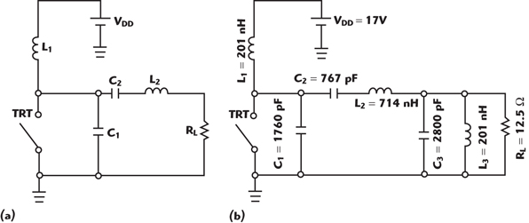
The figure shows a load network based on lumped elements that provides broadband operation for the class-E amplifier. It is derived from a bandpass filter with a first element shunt.9 This load network provides a complex load admittance at the fundamental and pure capacitive load admittance at harmonics over a broad bandwidth. The network is made of lumped elements but could be synthesized by any other technique suitable for a specific application, such as transmission lines, if the required load profile is provided. The component values shown in this figure were calculated for a specific amplifier that will be described later and obviously must be calculated in any other case.
Figure 6 shows the simulated output power and efficiency versus frequency obtained with HEPA Plus10 for the wideband class-E amplifier, using real components. The quality factor of the passive components is estimated to be Q = 125 for the inductances and Q = 1000 for the capacitors. The value of C1 has been decreased to accommodate the COSS of the transistor (International Rectifier IRLI530G), and the values of C3 and L3 have been slightly modified to absorb the imaginary impedance component of the ferrite loaded Ruthroff transmission line transformer used in the amplifier. It is important to note that, in wideband designs, the effects of components must be taken into account not only at the fundamental but also at least at the two first harmonics (2f0 and 3f0).
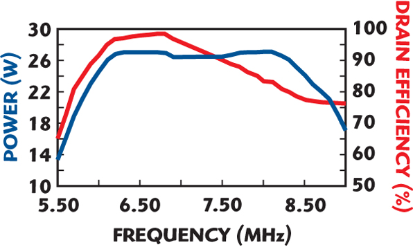
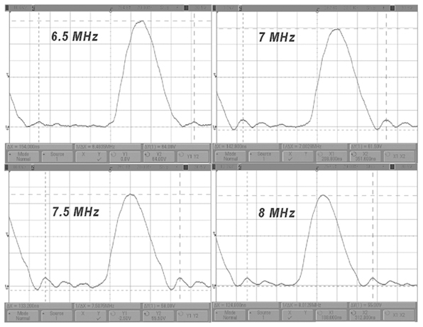
The actual measurements of output power POUT and drain efficiency of this amplifier are shown in Figure 7. The differences in output power and efficiency between measurements and simulations can be related to the losses in the transformer and printed circuit board besides imperfect component models and driving circuit. A slight frequency shift is also observed between the measured and simulated results, which is related to the proximity to the resonance frequency in some passive components that changes their low frequency value. The amplifier’s transistor drain-to-source waveforms were measured with a digital oscilloscope and are shown in Figure 8. These measurements show quasi-nominal class-E operation over the whole operating bandwidth of the amplifier.
Figure 9 shows a photograph of an amplifier embedded in an experimental HF EER communications transmitter. The high-Q air core silver-plated coils, high-Q porcelain capacitors and the 4:1 impedance Ruthroff transmission line transformer that converts the 50 Ω load into the 12.5 Ω required by the amplifier load network are clearly shown in the photograph besides the power transistor that requires only a copper polygon pad on the PCB to dissipate heat.
Conclusion
This work has shown that designing broadband high efficiency power amplifiers is possible using load-pull design techniques and synthesis of broadband load networks. This article is focused on the most popular high efficiency classes (D and E besides non high efficiency class-B), but the design principles explained here can be extended to the design of any broadband amplifier operating in any amplification class. Several simulations and measurements taken on a broadband class-E prototype have been shown to illustrate the effectiveness of this design technique.
The design methods shown in this article are devoted to the transistor output network, but the proper design of broadband high efficiency power amplifiers also requires efficient broadband drivers. This is not a trivial problem, especially at high frequencies and microwaves, and deserves further research.

Acknowledgment
The authors thank Nathan Sokal for his helpful discussions on this topic. This work was partially supported by Spanish MEC funding (TEC2006-08210).
References
1. N.O. Sokal and A.D. Sokal, “High Efficiency Tuned Switching Power Amplifier,” United States Patent 3,919,656, November 11, 1975.
2. S.C. Cripps, “High Efficiency RF Power Amplifier,” United States Patent 5,329,249, July 12, 1994.
3. F.H. Raab, “Class-E, Class-C and Class-F Power Amplifiers Based Upon a Finite Number of Harmonics,” IEEE Transactions on Microwave Theory and Techniques, Vol. 49, No. 8, October 1998, pp. 1462–1468.
4. H.L. Krauss, C.W. Bostian and F.H. Raab, Solid State Radio Engineering, John Wiley & Sons Inc., Hoboken, NJ, 1980.
5. H.O. Granberg, “Building Push-pull Multioctave, VHF Power Amplifiers,” Microwaves and RF, November 1987, pp. 77–86.
6. P.J. Baxandall, “Transistor Sine-wave LC Oscillators: Some General Considerations and New Developments,” Proceedings of the Institute of Electrical Engineering, part B, Vol. 106, May 1959, pp. 748–758.
7. N.O. Sokal and A.D. Sokal, “Class-E: A New Class of High Efficiency Tuned Single-ended Switching Power Amplifiers,” IEEE Journal of Solid-State Circuits, Vol. 10, No. 3, June 1975, pp. 168–176.
8. N.O. Sokal, Scalable Analog Circuit Design, High Speed D/A Converters, RF Power Amplifiers, Kluwer Academic Publishers, The Netherlands, 2002.
9. F.J. Ortega-Gonzalez, “Load-pull Wideband Class-E Amplifier,” IEEE Microwave and Wireless Component Letters, Vol. 17, No. 3, March 2007, pp. 235–237.
10. Design Automation Inc., 4 Tyler Road, Lexington, MA.