
Variations in semiconductor manufacturing technology are unavoidable; therefore, the IC must be designed for yield even at the extremes of process variation. The goal of statistical and corner models is accurate simulation of the process-induced variation of circuit performances, such as gain-bandwidth products, distortion levels and phase noise. Process control monitoring (PCM), performed on every wafer produced by a fab, measures the process variation of device-level electrical performances (Idsat, beta), referred to here as e. The statistical infrastructure called backward propagation of variance (BPV)1 produces statistical models that guarantee precise simulation of the variation of e and achieve the goal through the physical nature of the compact models. Therefore, a direct BPV requirement is scalable, physical compact models that accurately simulate the physical sensitivities of e to variations in process and geometry model parameters, termed p.
Figure 1 shows the mathematical representation of BPV in action for the PSP model. The variances of e are input directly from the PCM. The PSP sensitivity matrix is calculated directly within the circuit simulator. The system determines the variances of p (σ2δp), which guarantees alignment of the simulated and measured variances of e. The 1–σ values of p are then input to the Monte Carlo statistical simulation tool within the design environment or scaled to produce corner models. The results are accurate in most cases to < 0.5 percent. This technique is employed across all device types, utilizing all the available PCM. In addition to accurate simulation of individual e, physical correlations among multiple e are accurately captured. The BPV infrastructure is the basis for a suite of tools embedded in the Jazz analog design environment including X-Sigma models and the Process Control Modeling Tool (PCMT).
X-Sigma
As a greater amount of RF integrated circuits connect with consumer applications, the influence of “cycle time to functional silicon” on market penetration and ultimate product success is on par with—and in some cases exceeds—overall cost or performance. In many cases, front-end design consumes the bulk of the design cycle. While completing a design that meets specification for nominal process cases can be quick, the larger portion of budgeted cycle time is spent improving design robustness so target specifications are met across process variation. To allow for efficient process variation exploration, the proposed design flow offers designers a tool to help them understand how effectively the IC meets design targets across such variations. As motivation, take the example of a designer’s goal to meet specification targets across ±3σ process corners. ±3σ represents 99.7 percent of statistically expected process variation, which is close to ideal yield. As an example, it may require three design team weeks to achieve 95 percent (or ±2σ) spec coverage, but an additional eight weeks to reach ±3σ coverage. In consideration of time to market, the design team may want to trade off design cycle for a small percentage of corner compliance. Typical foundries provide hard coded ±3σ corner models, restricting information concerning the design’s location within the 3σ process variation space. The Jazz X-Sigma corner platform provides process sigmas as variable inputs that can be swept in an analog manner across the process variation spectrum. The added flexibility provides direct insight into circuit sensitivities across the process variation space previously hidden by the fixed corner settings. Through X-Sigma, the example design team may determine what coverage—and hence, expected parametric yield—a design will enjoy at any point in the design cycle. Figure 2 illustrates a sample X-Sigma corner-selection process for a given specification distribution.

Physical Design Enablement
The increase in carrier frequencies in microwave applications has made possible the cost-effective integration of active and passive microwave elements into a single substrate. In previous generations, the cost associated with introducing microwave compliant layouts into ICs was unreasonable because the performances (for example, inductance and impedance) resulted in prohibitive geometries. To illustrate, a quarter-wave transformer built on a microstrip for a 900 MHz spread spectrum application will be 70 times longer than its parallel for a 64 GHz band application such as collision avoidance. In modern technologies, it is now possible to integrate these high-value functionalities in a cost-effective manner. For active circuitry, the improvement in process technologies through scaling has also paved the way for ICs to reach performance previously only possible through higher-cost discrete systems. In order to manage the risk of introducing layout topologies with inherent microwave deficiencies, the physical design libraries include parameterized layout cells (pcells) with embedded process technology knowledge and best practices. Moreover, the physical views are robustly tied into the simulation environment in the same manner as the device models, enabling design performance optimization.
RF MOSFET
The role of the CMOS transistor as an RF capable device continues to expand across the industry. In order to obtain the required performance metrics, their physical implementation must be tailored to achieve maximum RF performance. Two key device parasitics to be minimized are gate and substrate resistance. Gate resistance is a critical component of device noise performance and its subsequent mapping to phase noise, linearity, etc. Minimizing these negative effects is possible through proper gate connectivity layout configurations. The design platform should include RF pcells allowing multiple FET gate configurations, driving down the total noise generating resistance intrinsic to the gate.9 At RF frequencies, the core device interacts with the lossy silicon substrate, directly reducing the output impedance. This interaction is heavily dependent on how the bulk ties are distributed around the device. In RF CMOS layout, bulk contacts closely wrapped around the device produce the smallest deviation from ideal behavior. The pcell should therefore also contain multiple substrate tie options, including a ring that significantly reduces the “rollup” in drain-source conductance gds at high frequencies. It is important to offer a parameterized cell that can draw these optimized contacts, but just as importantly drive the models that accurately capture the element configuration.
NPN
Bipolar devices, including high-performance silicon germanium NPNs, are common in high-performance RF applications due to their superior gain, noise, isolation and power metrics. Bipolar layout style strongly influences device performance; for this reason an RF focused parameterized NPN cell that yields high emitter area and low parasitic resistance and capacitance is requisite. As the cornerstone of the optimized NPN pcell, the emitter length should be offered as a fully scalable parameter. This feature, available in the Jazz Design Enablement, allows for the definition of arbitrary emitter areas, facilitating design for gain, noise, or matching. The NPN pcells allow designers to explore different base and collector topologies for further performance optimization. Some examples of available scaling features include:
• Base configuration: choose between single or dual base contacts to trade off parasitic capacitance/footprint for base resistance
• Collector configuration: choose between single or dual collector contacts to trade off collector resistance for parasitic capacitance/footprint. RF enhanced cell uses low resistance double collector contacts for multi-emitter devices
• Emitter width configuration: choose between emitter widths to trade off between base resistances, fT for parasitic capacitance, current consumption and matching
Inductor
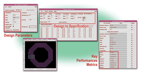
In electromagnetic elements, layout defines first-order device performance. The aforementioned JIT inductor toolbox provides scalable inductor and balun parameterized cells built upon electrical and process rules, metal current density limitations and process technology insight. To assist designers in selecting the appropriate passive on-chip component, an inductor library should provide designers with access to quality factor, inductance and frequency metrics prior to layout or simulations, as is the case with the JIT kit. This front-end design feature is combined with a fast-coil-optimization tool that helps designers quickly explore device geometry and electrical performance space. Figure 3 shows a sample inductor design flow using JIT.
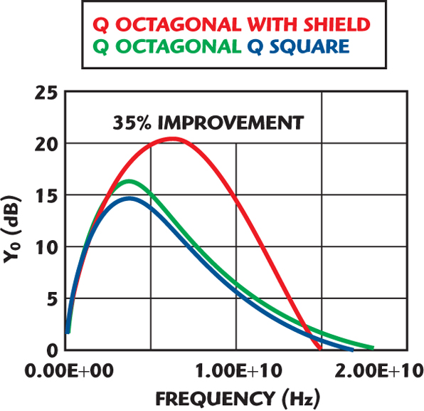
In all cases, these validated cells maximize performance without introducing costly modules, such as RDL layers or post processing. Figure 4 shows the Q performance comparison of square, octagonal and shielded octagonal geometries. Figure 5 illustrates the improved inductor isolation of a device over ground shield vs. a device over standard substrate.
Additional design flow features must include critical design rule requirements to safeguard modeled EM performance. For instance, cell integration prohibits running a symmetric inductor center tab through the core of the inductor as it would increase AC resistance and degrade Q. Another design rule may restrict the addition of dummy metal fill around the device, which would adversely affect performance. A smart library like JIT can enforce these restrictions or lift them for nanometer scale technologies where metal fill is required within inductors to meet manufacturing requirements.
DFM Loop Closure Tools
Statistical Loop Closure (SLC)

Successful RF analog design hinges on synergy between models and fab. Statistical-process-control tools such as Cp and Cpk measure precision and quality of the PCM data. Many PCM parameters vary independently, leading to straightforward mapping and verification of models, fab disposition limits and actual PCM data through Cp/Cpk targets. However, as previously described, many PCM parameters are derived from shared device and process elements leading to strong statistical PCM correlation. Producing a cohesive and accurate model-to-fab statistical platform is very challenging, and once achieved, needs continual verification. Statistical Loop Closure (SLC) is a DFM-driven methodology that provides a continuous-improvement quality assurance mechanism.
Figure 6 shows a sample output. The scatter plot compares statistical simulation outputs for two PCM parameters vs. the measured PCM equivalents. In this example, a SiGe NPN beta and breakdown voltage are compared. Confidence ellipses are added to illustrate statistical containment probability. The goal of statistical loop closure is to ensure the model and measured parameter correlations and containment ellipses forecast equivalent statistical performance. Beta and breakdown correlate owing to mutual dependence on base and collector doping. The example shows fab measurements running within specification limits and accurately correlated to the statistical model. The Jazz SLC environment is automated to compile monthly reports that include correlation metrics and to send alerts if unexpected drifts are detected.

PCMT
Closing the gap between simulation results and measured bench data is often the hardest step of a successful design cycle. Designers waste time and resources searching for the root cause of the measured deviations, increasing development costs and time to market. A robust analytical method to evaluate specific semiconductor samples is highly desirable. The Jazz PCMT produces models precisely aligned to the PCM data of a specific silicon sample through a modified statistical BPV engine previously described. PCMT enables insightful correlation of actual silicon IC measurements to circuit simulations, resulting in design optimization and cycle time reduction. PCMT is integrated into the designer wafer in process (WIP) web portal and produces model files easily integrated into the design environment. An example of how PCMT will adapt electrical parameters is shown in Figure 7 for NPN Beta and CMOS Idsat.
Conclusion

As the role of microwave circuits as a primary building block of communications systems has expanded into new industries and applications such as AIMS, the lines separating microwave and consumer commodity products have vanished. New breeds of microwave products leverage semiconductor technologies that decisively allow for integration of high-value functionality in a cost-effective manner. As these analog-only circuits evolve into integrated AIMS solutions, a design flow that delivers robust models and tools intimately tied to the manufacturing process is requisite in the pursuit of performance, manufacturability and optimal time to market. As an example of such a flow, the Jazz RF Analog Design Enablement has been presented as a state-of-the-art methodology that promotes the design of first-time-right optimized microwave modules. Examples of modeling methods, physical design and loop closure tools have been showcased as illustrations of design enablement. In addition to the presented examples, Jazz Semiconductor offers interconnect and substrate parasitic extraction, metal dummy modeling, analog DFM design rules and prefabrication yield estimation. The unique design enablement environment fosters the innovation of highly differentiated microwave technology.
References
• 1. C.C. McAndrew, “Statistical Modeling for Circuit Simulation,” 2003 Quality Electronic Design Proceedings, March 24–26, 2003, pp. 357–362.
• 2. G. Gildenblat, X. Li, W. Wu, H. Wang, A. Jha, R. Van Langevelde, G.D.J. Smit, A.J. Scholten and D.B.M. Klaassen, “PSP: An Advanced Surface-potential-based MOSFET Model for Circuit,” IEEE Transactions on Electron Devices, Vol. 53, Issue 9, September 2006, pp. 1979–1993.
• 3. N. Scheinberg and A. Pinkhasov, “A Computer Simulation Model for Simulating Distortion in FET Resistors,” IEEE Transactions on Computer-Aided Design of Integrated Circuits and Systems, Vol. 19, Issue 9, 2000, pp. 981–989.
• 4. Y. Han, L.E. Larson and D.Y.C. Lie, “A Low Voltage 12 GHz VCO in 0.13μ CMOS for OFDM Applications,” Silicon Monolithic Integrated Circuits in RF Systems Conference Proceedings, January 2006, pp. 379–382.
• 5. C. Changhua, Y. Ding and K.K. O, “A 50 GHz Phase-locked Loop in 130-nm CMOS,” IEEE 2006 CICC Proceedings, 2006, pp. 21–24.
• 6. M. Simon, P. Laaser, V. Filimon, H. Geltinger, D. Friedrich, Y. Raman and R. Weigel, “An 802.11a/b/g RF Transceiver in an SoC,” IEEE 2007 ISSCC Proceedings, 2007, pp. 562–622.
• 7. Z. Zhu, Q. Zhou, W. Wu, G. Gildenblat, Z. Yan, J. Cordovez, C. McAndrew, F. Anderson, J.C.J. Paasschens, R. van Langevelde, P. Kolev, R. Cherne and C. Yao, “PSP-based Scalable MOS Varactor Model,” IEEE Custom Integrated Circuits Conference 2007, September 16–19, 2007, pp. 495–502.
• 8. B. Razavi, RF Microelectronics, Prentice Hall, Upper Saddle River, NJ, 1998, p. 221.
• 9. V. Blaschke and J. Victory, “A Scalable Model Methodology for Octagonal Differential and Single-ended Inductors,” IEEE Custom Integrated Circuits Conference 2006, September 10–13, 2006, pp. 717–720.
• 10. G.A.M. Hurkx, P. Agarwal, R. Dekker, E. van der Heijden and H. Veenstra, “RF Figures-of-merit for Process Optimization,” IEEE Transactions on Electron Devices, Vol. 51, Issue 12, December 2004, pp. 2121–2128.