
Integration of RF power, RF small signal, digital, DC and supervision circuits is still one of the main goals of modern radar, satellite and wireless communications technology. Today’s solutions of close-to-antenna devices use a stack approach for integration of RF filters with power splitters/combiners and multilayer printed circuit boards (PCB) containing the rest of the circuitry.
One device that is difficult to integrate is a directional coupler mounted close to an antenna for the purpose of monitoring the transmitted and reflected powers. The requirements for such a coupler are of high importance: very low insertion loss, very good matching of the main line (carrying the power), sufficient power handling and a directivity better than 20 to 26 dB in both directions. Because the two coupled ports of the coupler are used simultaneously, there is no possibility to “improve” the directivity by tuning one of the coupled line ports. A modular approach is often implemented. This dictates that a high quality coupler would be placed separately, outside the integrated units, and connected utilizing cables or special transitions. This, of course, adds to the manufacturing cost as well as increases the number of steps in the process.
There are few known solutions allowing the partial integration of the coupler into the PCB. Four of them are patented1-4 and another one is offered by Teppati and Ferrero.5 Most of them are of the coaxial-to-stripline or coaxial-to-microstrip configurations, where the printed line is placed on top of the coaxial line. Persson4 uses a multilayer PCB configuration where both the main and coupled line are milled and suspended. The techniques used to compensate the coupler in order to achieve perfect matching and high directivity over a wide frequency range are not discussed in these publications. It is known6,7 that, assuming the validity of quasi-static approximation, asymmetrical couplers in inhomogeneous dielectric media can be compensated if the inductive and capacitive coupling coefficients are equalized and the coupled lines are terminated with the proper impedances:

inductive coupling coefficient
capacitive coupling coefficient
![]()
characteristic impedances of terminating lines

characteristic impedance of line i in the presence of line j (j = 1,2, j ? i)
Li,Ci, i = 1,2 = self-inductance and self-capacitance per unit length of line i in the presence of line j (j = 1,2, j ? i), respectively
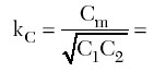
Lm,Cm = mutual inductance and mutual capacitance per unit length, respectively
The scope of this work was to identify a directional coupler structure having high power handling in the main line, being fully or partially embedded into the PCB, achieving a coupling coefficient in the range –20 to –40 dB, and being always theoretically compensated. Three examples of possible solutions are presented in Figure 1.8 The first structure shown is fully embedded into the PCB. The main line is suspended over the chassis and is composed of four printed strips connected by via-holes. The coupled line is hidden inside the PCB and can be treated as a stripline. The dielectric material is milled out in the vicinity of the main line and protrudes past the edges of the tuning ground planes (at a distance s2). The other structures shown are composed of a coaxial line (carrying the power) and a stripline or microstrip, as the coupled line, placed beside the coaxial line. In these structures, only the coupled line is embedded into the PCB. The dielectric material protrudes past the edge of the tuning ground plane(s), towards the center conductor of the coaxial line at a distance s2.

Fig. 1 Three cross-sections of novel asymmetrical directional coupler structures.
There are many possible modifications of the coupler topology using the proposed concept. Other cross-section shapes and locations of the main line, as well as modifications of the coupled line are possible. Generally, the structure should contain the low loss main line (embedded into the PCB, or not), the coupled line (embedded into the PCB), tuning ground plane(s) and the dielectric material of the PCB protruding past the edge of the tuning plane(s), towards the main line. These last two features are necessary to assure theoretical compensation of the coupler.
Areas of achievable coupling coefficients under the compensation conditions, dependence of the coupler directivity on the deviation from these conditions and structural parameters for realizing a –30 dB coupler in a variety of dielectric substrate permittivity are presented in the analysis section. Experimental results are presented for two –30 dB and –20 dB directional couplers and for a DC block integrated with a –30 dB coupler.
Analysis
The analysis of the proposed structures was performed using a static 2-D solver.9 The transversal geometrical dimensions of the 50 ? matched directional couplers were calculated as a function of the dielectric substrate protrusion distance s2, and changes to the inductive kL and capacitive kC coupling coefficients were observed. Most of the calculations were carried out for the FR-4 Matsushita, halogen-free, substrate material. The results of the calculations for the fully embedded structure are presented in Figure 2. It is clear that this structure can be compensated in the range of coupling coefficients from –40 to –20 dB by changing the distance s1 between the main line and the coupled line along with adjusting distance s2. The widths of the main (w2) and the coupled (w1) lines vary from 5.5 to 5.4 mm, and from 1.5 to 0.5 mm, respectively.

Fig. 2 Inductive and capacitive coupling coefficients versus s2 for the fully embedded structure.
The results shown in Figure 3 were obtained for the structure using a coaxial main line and a stripline coupled line with a modified outer ground enclosure. It is shown that even “pure air” and “pure stripline” coupled transmission lines can be compensated in spite of large difference between the values of effective dielectric permittivity of the two orthogonal modes propagated in the structure. This feature distinguishes the asymmetrical coupled lines from the symmetrical lines. The latter ones are compensated if values of these permittivities are equal. Results of computations for the third structure, using a coaxial main line and a microstrip coupled line, are shown in Figure 4. The coupling level can be adjusted in this structure not only by changing the distance between the coupled lines (s0 + s1) but also by changing the suspension level h2 of the PCB — the higher this suspension, the weaker the coupling. The effect of deviations from the compensation conditions on the directivity of the coupler is also shown. Tighter tolerances on the distance s2 are needed for higher suspended PCBs.

Fig. 3 Modified coaxial-to-stripline structure; (a) geometry, (b) inductive and capacitive coupling coefficients and (c) effective dielectric constant for two orthogonal modes.

Fig. 4 Coaxial-to-microstrip structure; (a) coupling coefficients and (b) corresponding directivity of the coupler.
The structural dimensions of a –30 dB, 50 W matched, compensated coupler, with varying dielectric permittivity of the microstrip substrate, are given in Figure 5. These curves are very convenient for a practical realization using any chosen PCB dielectric material. The dielectric material protrusion distance s2 varies more dramatically in the region of low dielectric constant.

Fig. 5 Dimensions of the 50 W matched coaxial-to-microstrip coupler versus dielectric constant of the PCB.
It has been shown that coupling coefficients in the range of –20 to –40 dB are easily achievable with the proposed structures. These coupling levels can be realized with convenient structural dimensions, meaning that the proposed structures are not sensitive to dimensional tolerances.
Experimental Results
A –30 dB directional coupler was designed and manufactured in the fully embedded configuration. Layouts of the first and third PCB layers are shown in Figure 6. The copper pattern on the second and the fourth layer is similar to the first one, except for the microstrip lines connecting the coupled line to the edge of the PCB. The measured results are presented in Figure 7. The coupling level at the mid-band frequency is exactly as predicted in the design. The main suspended line is perfectly matched — the return loss is better than 30 dB. The directivity exceeds 25 dB in the entire frequency band presented, and follows the return loss of the rather poorly matched coupled line, which is affected by the stripline to microstrip and microstrip to SMA connector transitions.

Fig. 6 Layout of the first and third layers of the –30 dB fully embedded directional coupler.

Fig. 7 Measured responses for the -30 dB directional coupler.
A –20 dB directional coupler was designed and manufactured utilizing the coaxial to microstrip configuration. A photograph of this coupler and the measurement results are shown in Figures 8 and 9, respectively. Small manual adjustments have been done to obtain optimal chamfering of the 90° microstrip bends. This has led to improvements in the microstrip line matching and also in isolation. The directivity of the coupler is better than 20 dB for frequencies up to 2.7 GHz and exceeds 30 dB in the 1.4 to 2.3 GHz frequency range. The visible directivity degradation above 2.7 GHz can be affected by the dispersion of the microstrip line, which is printed on a 1.7 mm thick substrate.

Fig. 8 The -20 dB coaxial-to-microstrip directional coupler.

Fig. 9 Measured response of the -20 dB directional coupler.
The fully embedded configuration is very convenient for further integration of other devices/circuits, commonly used close to the antenna port, such as a DC block or a lightning protection circuit. Using this configuration, a DC block was designed together with the power and antenna control –30 dB directional coupler. Layouts of the first and the third PCB layer are shown in Figure 10. The slots and isolated via-holes in the main line are easily visible. The measurement results are shown in Figure 11. The DC block is very well matched and has an insertion loss below 0.1 dB in the frequency band from 0.6 to 2.5 GHz. The center frequency for the DC block is shifted down 0.2 GHz compared to expectations because of the static design. The measured coupling value is less than the designed one by 0.3 dB. The directivity of the coupler is better than 25 dB throughout the whole frequency band presented, despite the poorly matched coupled line.
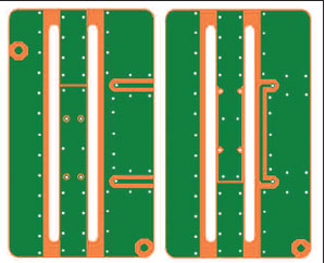
Fig. 10 Layout of the first and third layers of a DC block integrated with a fully embedded -30 dB directional coupler.

Fig. 11 Measured response of the -30 dB directional coupler with an integrated DC block.
These measurement results are remarkably good, which means that the quasi-static design can be used as a reliable starting point for a full-wave design. Some corrections should be considered, especially for higher frequency designs, due to discontinuities.
Conclusion
The various structures of directional couplers investigated in this article seem to be very promising for the sampling of forward and reflected RF power simultaneously. They allow the integration of RF power and small-signal parts of a device into a single unit. The required range of coupling coefficients from –20 to –40 dB is easily realizable. Very low insertion loss of the main line, wide bandwidth and good directivity are easily achieved. The insertion loss of the main line is additionally diminished due to the shorter length of the coupler compared to air solutions. This length is reduced approximately by a (1 + ??effc) factor, where eeffc is the effective dielectric constant for the mode associated with the coupled line, embedded in the dielectric material of the PCB, or printed on a dielectric board. The quasi-static design, presented in the article, makes an effective design possible based on the equalization of inductive and capacitive coupling coefficients.
References
1. “Coupleur Directif Entre Ligne Coaxiale et Ligne Triplaque,” Patent FR 1191414, 1959.
2. S. Jansson, “Breitseiten-Richtkoppler in Streifenleitungs-technik,” Patent DE 2320458, 1974.
3. Y. Fujihashi and Y. Oosumi, “Directional Coupler,” Patent JP 2003032013, 2003.
4. G. Persson, “Directional Coupler for High Power RF Signals,” PCT Patent Application, December 1997.
5. V. Teppati and A. Ferrero, “A New Class of Non-uniform, Broadband, Non-symmetrical Rectangular Coaxial-to-microstrip Directional Couplers for High Power Applications,” IEEE Microwave & Wireless Components Letters, Vol. 13, No. 4, April 2003, pp. 152–154.
6. T. Emery, Y. Chin, H. Lee and V.K. Tripathi, “Analysis and Design of an Ideal Non-symmetrical Coupled Microstrip Directional Coupler,” 1989 IEEE MTT-S International Microwave Symposium Digest, pp. 329–332.
7. K. Sachse, “The Scattering Parameters and Directional Coupler Analysis of Characteristically Terminated Asymmetric Coupled Transmission Lines in an Inhomogeneous Medium,” IEEE Transactions on Microwave Theory & Techniques, Vol. 38, No. 4, April 1990, pp. 417–425.
8. J. Dabrowski and A. Sawicki, PCT Patent Applications, filed April 2003 and April 2004.
9. A.R. Djordjevic, M.B. Bazdar, T.K. Sarkar and R.F. Harrington, LINPAR for Windows: Matrix Parameters for Multiconductor Transmission Lines, Software and User’s Manual, 2.0 ed., Artech House Inc., Norwood, MA, 1999.