
The gigahertz era in consumer electronics has catalyzed the convergence of RF and microwave applications with mainstream large-scale semiconductor technology. This merging of technology has brought performance, manufacturability and time-to-market requirements into the forefront of a world once driven solely by design-to-specification. Stand-alone microwave circuits are rapidly moving to analog intensive mixed-signal (AIMS) microwave ICs. Not too long ago, the quick manufacturing cycles of III-IV technologies allowed for countless fabrication iterations of microwave designs before reaching final design and subsequent mass production. These iterations were carried out in prototype vehicles that included tens of individually tweaked versions of a single IC. Later rather than sooner, one of the versions would function, and be selected for production. As these products are plugged into larger scale integrated chips, the high development cost and cycles associated with these technologies make it difficult to survive using this shotgun approach.
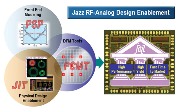
When microwave circuits enter the mixed-signal world, they must adapt to function in the mixed-signal process technology. For this adaptation to be successful, the design flow must facilitate the design of optimized microwave modules with the available technology. Figure 1 displays Jazz RF Analog Design Enablement, a novel design platform that delivers robust models and design tools intimately tied to the manufacturing process directly to the IC designer’s desk. Application of design enablement to the RF and microwave design space facilitates the innovation of highly differentiated products. The flow starts with a physical, scalable modeling platform combined with a robust statistical infrastructure to simulate design sensitivity to process variation, thus enabling first-time-right semiconductors. The modeling platform resides in a leading commercial IC design environment, which provides scalable parameterized cells for all components with embedded process technology knowledge, facilitating direct design space exploration and optimization. Finally, tools for final loop closure between fabricated silicon and simulation provide a feedback mechanism for continual design improvement.
Front End Design Enablement: Modeling Methodology
The RF IC designer creates a highly complex integrated circuit, which executes complicated functions at various levels of the system. In the end, regardless of the level of abstraction in which an RF system is defined, the semiconductor transistors and integrated passives do the work. Thus, the designer needs to know how these devices perform, in particular how they respond to electrical, magnetic and thermal stimuli. Device models provide this information to the designer. One can think of models as the prescription glasses a designer must be fitted with before the IC design process commences. Different technologies such as RFCMOS, SiGe BiCMOS, or GaAs come with a different prescription, enabling a designer to understand the process and thus make decisions on how to design the particular IC.
An accurate modeling platform consists of a set of physical compact models that are accurately characterized to the semiconductor technology and, just as importantly, are readily available within the IC design environment. The models must not only reflect the nominal process, but also accurately predict the natural process variation of semiconductor technology. All production IC designs are ultimately subject to the semiconductor manufacturing process variation over the life of the product. Hence, the design must be robust and meet performance specifications, or “yield,” across the entire process variation space. Therefore, statistical models representing the process variation of the technology must be available within the design environment.
Physical Compact Modeling
A compact model is a set of analytical equations that describe the electrical, electromagnetic and thermal behavior, implemented in a SPICE-like simulation tool. The models make necessary simplifications from the full physics while retaining sufficient accuracy and reasonable simulation times. As a somewhat simplified assertion, one can state that the simulation time is directly proportional to the complexity of the model. Consequently, the best compact models contain simplifications that retain accuracy while improving speed.
Physically based compact models are based on the fundamental process parameters that control the device behavior, such as oxide thickness for the MOS devices and base doping for an NPN. Additionally, compact models should be formulated based on the geometrical variables including scalable design parameters and process design rules. Examples of scalability include gate length and width of a MOSFET or GaAs FET, emitter length and width of bipolars, and inductor line widths and number of turns. Examples of process design rules include poly to contact, deep trench and active area spacing.
Compact models should be C∞ continuous over the entire operating range of a device, where Cn continuous means the function and its nth order derivatives are continuous as described by McAndrew.1 Additionally, models should provide correct asymptotic behavior to the extremes of input stimulus such as voltage or temperature. Such requirements ensure robust simulation convergence behavior and model accuracy in regions not measured during model characterization.
As semiconductor technology has advanced, so has compact modeling. Modern day compact models meet all the requirements previously mentioned providing robust simulation performance and accuracy. Examples of three advanced, state-of-the-art compact models (PSP, MOSVAR and JIT ), offered as part of the Jazz Analog Design Environment, are highlighted next.
PSP
The PSP model, the next generation standard compact MOSFET model, is an advanced surface potential-based model geared towards 90 nm and below technology nodes.2 Furthermore, the PSP model remedies many issues with the well-known prior generation model BSIM, making it quite effective for older technologies such as 0.18 μm. PSP provides the best model for RF analog design through complete physical treatment of noise sources including gate and channel noise correlation, and continuous high order derivatives crucial for distortion analysis. An example of the effectiveness of the PSP model for distortion simulation is presented here.
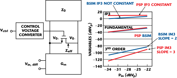
There are several RF circuit blocks that utilize the MOSFET in a passive context such as passive mixers and RF attenuators. Figure 2 shows a simplified diagram of an RF attenuator based on a transconductance amplifier configuration, a circuit block commonly used in RF transceiver design. The GM block combined with the load impedance Z0 sets the attenuation or gain of the block. A common and effective design technique utilizes an NFET hooked with the drain and source across the differential output signal, DC biasing the device at Vds = 0. The gate voltage is then controlled through automated gain control (AGC) circuitry to modulate the channel resistance, changing the effective load impedance Zeff, thus modulating the attenuation (or gain) of the block. The figure also shows intermodulation distortion simulations for the attenuator, based on the PSP and BSIM MOSFET model. At low input power levels, the third harmonic (IM3) must exhibit a slope of three based on harmonic power series analysis. The BSIM model simulates a slope of two, which is physically incorrect and leads directly to incorrect simulation of third-order intermodulation distortion, or IP3 analysis. By contrast, PSP exhibits the correct slope of three for IM3 and thus the expected IP3 results.

At the very root of this problem is the discontinuity of the high order derivatives at the Vds = 0 point in the BSIM model.3 Figure 3 shows the results of the well-known Gummel symmetry tests for a NFET in the Jazz SiGe/RFCMOS SBL13 0.13 μm technology. The NFET is swept symmetrically across the Vds = 0 point, with the drain current and the third derivatives plotted. The clear third derivative discontinuity in the BSIM model produces the IIP3 slope = 2. PSP displays not only continuous behavior at the third derivative, but tracks the data very reasonably. An RF designer can then design such a key block and others that depend on the accuracy around the Vds = 0 point such as RF passive mixers and switches with a high degree of confidence.
MOSVAR
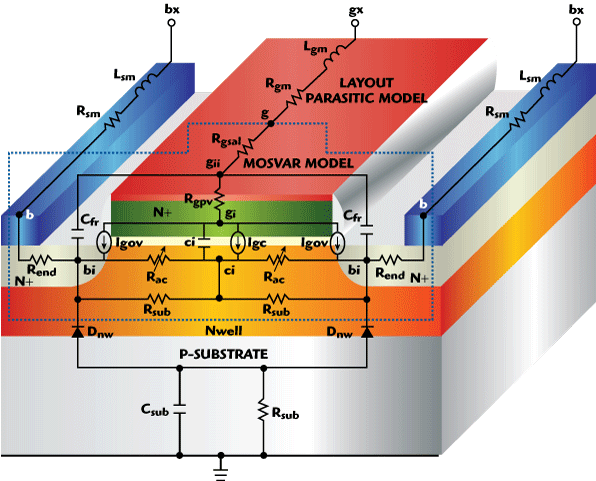
Design of RF/analog and millimeter wave circuits requires accurate, scalable compact models not only for the active transistors but, just as critically, the passive components in a given technology. This includes the MOS varactor, which provides frequency tuning for circuits such as voltage-controlled oscillators (VCO). VCOs provide frequency synthesis and system timing in many modern day RF systems, such as WLAN, WiMAX, UWB, automotive radar and high speed optical communications systems.4,5,6 The recently developed MOSVAR model shown in Figure 4 is a physically based scalable model for MOS varactors.7 The model includes a PSP-based analytical surface potential charge formulation and physical geometry and process parameter-based parasitic modeling. The model provides highly accurate simulations of key varactor performances such as capacitance and quality factor Q over voltage, frequency and geometry. Above all, the model provides the physical insights to the designer, enabling design trade-offs such as phase noise vs. oscillator gain.
In a typical VCO tank circuit, an integrated inductor (L) and a MOS varactor (C) set the oscillation frequency. The tank quality factor (Qtank), which directly affects the VCO phase noise, is given by

derived using the approximations for the tank components:

RX (where X denotes L or C) is the resistive loss for each component in the series tank path. Equation 1 shows that at low frequencies, Qtank is controlled by the inductor while at high frequencies Qtank is controlled by the MOS varactor. Leeson’s phase noise model8 provides direct insight into the varactor impact on phase noise (PN). It relates the PN transfer function H(j Δω) to the oscillator parameters by

where ω = oscillator center frequency
Δω = offset frequency where the phase noise measurement is taken
At frequencies where QC dominates Equations 1 and 3 show that 
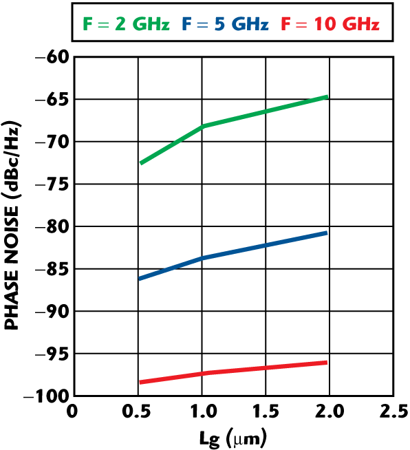
Figure 5 shows PN simulations of the VCO with the MOSVAR model.
PN increases with Lg, as expected due to the increased RC from the Nwell resistance. In addition, dPN/ dLg increases at higher frequencies above 5 GHz due to the increased influence of QC compared to QL. The physical, scalable nature of the MOSVAR model provides direct insight into the MOS varactor influence on PN with respect to frequency and geometry, facilitating design of stringent RF and millimeter-wave VCO design criteria such as low phase noise.
Jazz Inductor Toolbox (JIT)
In addition to providing the complimentary tank element to the varactor in VCOs, integrated inductors and baluns are key components to RF and millimeter design where they are heavily used in filtering and impedance matching applications. The Jazz Inductor Toolbox (JIT) provides a comprehensive inductor design environment including scalable compact models and parameterized layout cells, delivering a turnkey design solution to the IC designer.9 JIT feeds the technology parameters (for example, metal sheet resistance, interlayer dielectric thickness and substrate resistance) directly into a set of comprehensive analytical equations for the self and mutual inductance, parasitic resistance including high frequency skin effects and capacitance. The general void of this in the industry often leaves designers to custom inductor design through a time-consuming iterative process of EM simulation and/or silicon verification.

This inductor toolbox provides a comprehensive, scalable library of inductors applicable to a large design space. The library includes conventional single-ended spirals common to filtering and impedance matching in power amplifiers. Symmetrical inductors enable the use of differential circuit design, well-known to produce improved linearity, noise immunity and common mode rejection ratio (CMRR) in transceiver design. Supported inductor styles include octagonal geometries, which enhance Q performance through reduction in parasitic resistance and capacitance. Additionally, scalable patterned ground shields provide additional Q boost combined with enhanced noise isolation critical to RF systems. Figure 6 shows a microscope photograph of a symmetric inductor over a ground shield. Designers can also leverage a scalable passive library for characterization of transmission lines and other components such as tees and bends. As the infrastructure includes high frequency effects, the broadband output models produce low risk and rapid RF design validation.
Conclusion
In the first part of this series, the role of microwave circuits as primary building blocks of communications systems and their expansion into new industries and applications such as AIMS is considered. We examined how the lines separating microwave and consumer commodity products have vanished. Under these conditions, new breeds of microwave products are leveraging semiconductor technologies that decisively allow for integration of high value functionality in a cost-effective manner. As these analog-only circuits evolve into integrated AIMS solutions, a design flow that delivers robust models and tools intimately tied to the manufacturing process is requisite in the pursuit of performance, manufacturability and time-to-market. As an example of such a flow, the Jazz RF Analog Design Enablement has been presented as a state-of-the art methodology that promotes the design of first-time-right optimized microwave modules. In the second part of this series, examples of modeling methods, physical design and loop closure tools will be showcased as illustrations of design enablement.
References
1. C.C. McAndrew, “Statistical Modeling for Circuit Simulation,” Quality Electronic Design, 2003 Proceedings, Fourth International Symposium, March 2003, pp. 357–362.
2. G. Gildenblat, X. Li, W. Wu, H. Wang, A. Jha, R. Van Langevelde, G.D.J. Smit, A.J. Scholten and D.B.M. Klaassen, “PSP: An Advanced Surface-potential-based MOSFET Model for Circuit Simulation Electron Devices,” IEEE Transactions, Vol. 53, Issue 9, September 2006, pp. 1979–1993.
3. N. Scheinberg and A. Pinkhasov, “A Computer Simulation Model for Simulating Distortion in FET Resistors,” Computer-Aided Design of Integrated Circuits and Systems, IEEE Transactions, Vol. 19, Issue 9, September 2000, pp. 981–989.
4. Y. Han, L.E. Larson and D.Y.C. Lie, “A Low Voltage 12 GHz VCO in mCMOS for OFDM Applications ±0.13,” Silicon Monolithic Integrated Circuits in RF Systems Conference Proceedings, January 2006, pp. 379–382.
5. C. Changhua, Y. Ding and K.K. O, “A 50 GHz Phase Locked Loop in 130-nm CMOS,” Proc. IEEE 2006 CICC, 2006, pp. 21–24.
6. M. Simon, P. Laaser, V. Filimon, H. Geltinger, D. Friedrich, Y. Raman and R. Weigel, “An 802.11a/b/g RF Transceiver in an SoC,” Proc. IEEE 2007 ISSCC, 2007, pp. 562–622.
7. J. Victory, Z. Zhu, Q. Zhou, W. Wu, G. Gildenblat, Z. Yan, J. Cordovez, C. McAndrew, F. Anderson, J.C.J. Paasschens, R. van Langevelde, P. Kolev, R. Cherne and C. Yao, “PSP-based Scalable MOS Varactor Model,” 2007 IEEE Custom Integrated Circuits, September 2007, pp. 495–502.
8. B. Razavi, RF Microelectronics, Prentice Hall, Upper Saddle River, NJ, 1998.
9. V. Blaschke and J. Victory, “A Scalable Model Methodology for Octagonal Differential and Single-ended Inductors,” 2006 IEEE Custom Integrated Circuits September 2006, pp. 717–720.
10. G.A.M. Hurkx, P. Agarwal, R. Dekker, E. van der Heijden and H. Veenstra, “RF Figures-of-merit for Process Optimization,” Electron Devices, IEEE Transactions, Vol. 51, December 2004, pp. 2121–2128.