
Communication systems in the RF band are becoming bandwidth limited. Thus, the providers of communication systems have become interested in the X-/Ku-band for the next-generation of terrestrial systems, such as satellite communications, wireless local area networks (WLAN) and local multipoint distribution systems (LMDS). The performance of high power amplifiers (PA) has been drastically improved on GaAs-based PHEMT MMICs. Moreover, the superior performances of InP-based PHEMTs can be improved significantly in satellite communication applications.
CPW MMIC power amplifiers are usually adopted for use in transmitter communication systems.1–3 Advantages in the novel CPW structures include the fact that the ground plane is placed on the top surface of the substrate, making the backside process unnecessary. Also, the ground planes between the CPW lines provide good isolation, which permits a compact circuit layout.

A high output power, with good thermal properties, was demonstrated in a number of microstrip MMIC amplifiers. On the contrary, the CPW structure was hardly used in power microwave applications, due to the poor power handling capability, which resulted from the high thermal resistance of the thick GaAs substrates and the elimination of the backside processing.4 The backside fabrication contributes the heat removal in microstrip-based circuits significantly, and offers a higher power performance. However, the CPW technology can be made compatible by utilizing modern packaging techniques, such as flip-chip bonding, and also provides a cost-effective solution for GaAs MMIC fabrication.
In this article, the characteristics of an X-/Ku-band PA are presented, which uses a two-stage amplifier and a CPW structure in InGaP/InGaAs E-mode PHEMT technology. The amplifier is designed to fully match the 50 Ω input and output impedances without any external circuit, and exhibits a maximum output power of 20.7 dBm and a linear power gain greater than 20 dB, which is appropriate for microwave power integrated circuits.
Design and Simulation of the CPW MMIC Amplifier

Figure 1 shows the schematic of the PA with the three-stage matching networks: input port, inter-stage and output port. The PA is designed as a two-stage, single-ended amplifier, in order to fully match to a 50 Ω impedance. First, the output matching network was designed for maximum output power and associated power efficiency in a 50 Ω load. The inter-stage network was then optimized to reduce the mismatching loss in the PA circuit; the output of the driver stage was matched to the input of the output-power stage. Finally, the input network matching was designed to achieve a uniform small-signal gain, and to improve the impedance matching for the proper input return loss. A conservative driver stage gain was chosen to ensure enough power to drive the output-power stage and to allow for process variations.
An instability resulted from the CPW discontinuities and electromagnetic (EM) effects in the power circuit, caused by the various components coupling at high frequencies. It was beneficial that all passive components were evaluated by an EM field simulator.5 Therefore, a circuit stability analysis was executed for each stage, in order to ensure having a sufficient margin in the X-/Ku-band. The gate resistors of each stage were also adjusted to improve the stability of the CPW power amplifier.6 Consequently, the circuit parameters optimization and EM simulation based on these essential matching networks were performed, so as to achieve the required circuit performance.

The CPW was designed with a narrow size width = 20 μm and gap = 10 μm, to reduce the excitation of parallel-plate modes7 and to eliminate discontinuity effects. Capacitors and resistive loading were used to prevent oscillations at low frequencies. The amplifier design eventually achieved unconditional stability over the whole X-/Ku-band. The S-parameters and power gain were simulated using the Advanced Design System (ADS). Figure 2 shows the simulated output power, gain and power-added efficiency (PAE) at 12 GHz and Vds = 4 V. It also shows that the 1 dB compression power points (P1dB) at the input and output are 0 and 19.2 dBm, respectively. The maximum power of this amplifier was approximately 21.8 dBm in the saturation region, with a maximum PAE of 25.5 percent.
Device Structure and CPW Power Amplifier MMIC Fabrication
For PHEMT fabrication consideration, the InGaP/InGaAs E-mode PHEMT offers an excellent selective etching for the gate recess between InGaP and GaAs, which increases the device yield in mass production. Furthermore, InGaP does not form DX-centers, which cause less deep level defects. Consequently, the InGaP/InGaAs GaAs substrate exhibits great potential to improve the reliability of the GaAs PHEMT MMIC.

Figure 3 shows the epitaxial structure of the In0.5Ga0.5P/In0.24Ga0.76As E-mode PHEMT, which is a sandwich PHEMT structure for high power consideration. The structure includes the double Si planar δ-doping layers, which sandwich the InGaAs undoped channel layer with AlGaAs spacer layers for high transconductance consideration. An undoped 100 Å InGaP Schottky layer was grown on an intrinsic GaAs to form a Schottky layer. Finally, two n+–GaAs cap layers were grown to improve the ohmic contact’s resistivity. The designed structure demonstrated a sheet charge density of 2.2 x 1012 cm–2 together with a Hall mobility of 6120 cm2/V-sec at 300 K after removing the n+–GaAs cap layer. In the device fabrication, the Au/Ge/Ni/Au ohmic contacts were deposited by e-beam evaporation and patterned by a conventional lift-off process. An ion-implant isolation technology was applied for mesa isolation to avoid sidewall gate leakage current.
After the high selectivity succinic acid gate recess process,8 the 0.15 μm gate metals Pt/Ti/Au (40 Å/500 Å/4000 Å) were deposited by a lift-off process. Typical DC drain-to-source current (Ids) versus drain-to-source voltage (Vds) characteristics of the fabricated InGaP/InGaAs E-mode PHEMT are shown in Figure 4. As can be seen, the device can be operated with a gate voltage up to 1.4 V, which corresponds to an Ids of 230 mA/mm when the drain voltage is 3 V. The Vgs dependence of transconductance (gm) and Ids at Vds = 2 V are also shown.
The threshold voltage (Vth) is 0.34 V (defined as Ids = 1mA/mm) and the maximum Ids and gm are 235 mA/mm and 390 mS/mm, respectively. In addition, the matching inductors and MIM capacitors were also achieved during the circuit fabrication. Therefore, the two-stage power amplifier MMIC was realized with an InGaP/InGaAs E-mode PHEMT technology. A microphotograph of the two-stage CPW PA MMIC, with a chip area of 2.3 x 0.87 mm, is shown in Figure 5.
Measured Power Results

The S-parameter measurements were performed with an Agilent 8510C vector network analyzer. The total DC power consumption of the amplifier was 780 mW, which included an Ids of 66 mA and Vds of 4 V for the driver stage (gate width = 2 fingers x 100 μm), and an Ids of 129 mA and Vds of 4 V for the output power stage (gate width = 4 fingers x 100 μm).
Figure 6 shows the small-signal gain (S21) of 17.6 dB, the input return loss (S11) of 18 dB and the output return loss (S21) of 7 dB at 12 GHz. Figure 7 shows the on-wafer measured output power, gain and PAE at Vds = 4 V, Ids = 209 mA and 12 GHz. The P1dB was attained at approximately 18.6 dBm, the saturated output power was achieved with 21 dBm and the maximum PAE was obtained at 18.3 percent for Pin = 8 dBm.
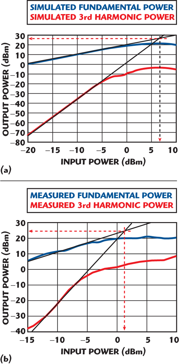
The third-order intercept inter-modulation (IP3) describes the nonlinearity of the circuit. In other words, when a two-tone input signal is fed to the amplifier, it will produce power at the fundamental frequencies and high order harmonic inter-modulation products. Consequently, a two-tone evaluation was performed at frequencies of 12.000 and 12.001 GHz, which were mixed to produce inter-modulation products in the power amplifier.
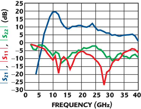
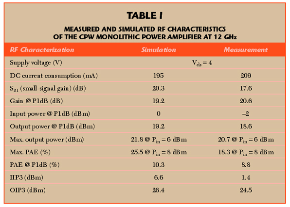
Figure 8 shows the comparison between the simulated and measured IP3. The simulated input third-order intercept point (IIP3) is 6.6 dBm and the output third-order intercept point (OIP3) is 26.4 dBm. The measured IIP3 and OIP3 are 1.4 and 24.5 dBm, respectively. Table 1 compares the simulated and measured RF characteristics of the amplifier. These power characterizations revealed a little inconsistency between the simulated and measured performance. The input return loss (S11) was poorer than expected. This result might be caused by fabrication variations, such as the elimination of backside via-hole processing. However, this CPW PA exhibits favorable RF characteristics in the X-/Ku-band and demonstrates that the InGaP/InGaAs E-mode PHEMT technology is an excellent approach.
Conclusion

In this article, a two-stage MMIC power amplifier, using an InGaP/InGaAs E-mode PHEMT technology and CPW topology, has been demonstrated. It exhibits an appropriate RF performance in the X-/Ku-band. The MMIC power amplifier gives an output power of 18.6 dBm, a linear power gain of approximately 20 dB and an output third-order intercept point (OIP3) of 24.5 dBm. The overall power characteristics exhibit high gain and linearity at 12 GHz. In summary, this CPW power amplifier has favorable RF characteristics and is very suitable for X-/Ku-band microwave integrated circuit power transmission applications.
Acknowledgments
The authors gratefully acknowledge the help in the power measurements by Jun-Nan Wang, who studied in the department of electronic engineering, Chang Gung University, and the National Chip Implementation Center (CIC). Additional thanks are extended to WIN Semiconductors Corp. for circuit fabrication.
References
1. T. Hirota, Y. Tarasawa and H. Ogawa, “Uniplanar MMIC Hybrids—A Proposed New MMIC Structure,” IEEE Transactions on Microwave Theory and Techniques, Vol. 35, No. 6, June 1987, pp. 576–581.
2. M. Muraguchi, T. Hirota, A. Minakawa, K. Ohwada and T. Sugeta, “Uniplanar MMICs and Their Applications,” IEEE Transactions on Microwave Theory and Techniques, Vol. 36, No. 12, December 1988, pp. 1896–1901.
3. M. Riaziat, I. Zubeck, S. Bandy and G. Zdasiuk, “Coplanar Waveguides Used in 2 to 18 GHz Distributed Amplifier,” 1986 IEEE MTT-S International Microwave Symposium Digest, pp. 337–338.
4. P. Cameron, W. Pan, C. Hanz and R. Nicklaus, “A Flip-chip High Efficiency X-band HPA,” 1997 IEEE MTT-S International Microwave Symposium Digest, Vol. 2, pp. 889–892.
5. M.H. Murgulescu, A. Boulouard, M. LeRouzic, P. Legaud, E. Penard and T. Zaquine, “38 GHz Coplanar Waveguide GaAs MMIC Amplifier,” Electronics Letters, Vol. 30, No. 21, 13 October 1994, pp. 1768–1770.
6. J.J. Komiak, S.C. Wang and T.J. Rogers, “High Efficiency 11 W Octave S/C-band PHEMT MMIC Power Amplifier,” 1997 IEEE MTT-S International Microwave Symposium Digest, Vol. 3, pp. 1421–1424.
7. M. Riaziat, R. Majidy Ahy and I.J. Fenc, “Propagation Modes and Dispersion Characteristics of Coplanar Waveguides,” IEEE Transactions on Microwave Theory and Techniques, Vol. 38, No. 3, March 1990, pp. 245–251.
8. H.C. Chiu, C.S. Cheng and Y.J. Shih, “High Uniformity Enhancement- and Depletion-mode InGaP/InGaAs PHEMTs Using Selective Succinic Acid Gate Recess Process,” Semiconductor Science and Technology, Vol. 21, 2006, pp. 55–59.

Chia-Song Wu received his MSEE degree from Tsing Hua University, Hsinchu, in 1985, and his PhD EE degree from National Central University, Chungli, Taiwan, in 1998. In 1986, he joined the Chung Shan Institute of Science and Technology (CSIST), where he focused on infrared detector technology. In August 2003, he joined the EE department of Vanung University and currently performs research on microwave and millimeter-wave integrated circuits. His research interests include OEIC and MMIC, such as laser diode, sub micron technology, microwave, millimeter devices and MMIC.

Hsien-Chin Chiu received his BS and PhD degrees in electrical engineering from National Central University, Chungli, Taiwan, in 1998 and 2003, respectively. In 2003, he joined Win Semiconductors Corp., Tao Yuan, Taiwan, where he was engaged in the research and development of six-inch GaAs PHEMTs and related integrated circuits. In June 2004, he joined the faculty of the EE department at Chang Gung University and focused on microwave, millimeter-wave integrated circuits, fiber communication circuits and nanotechnology. His research interests include deep submicron electron-beam lithography, solid-state physics, compound semiconductors, microwave, millimeter devices and integrated circuits.