
With the continuous trend to reduce the size of electronic modules and increase the integration levels, the integration of passive elements within the interconnection board or substrate becomes more and more a key factor. In addition to size reduction, passive integration leads to assembly cost reduction as well as potential module reliability improvements.
Among different substrate technologies, low temperature co-fired ceramic (LTCC), which offers performance suitable for RF and microwave applications, features unique capabilities with regard to passive integration. This article reports the evaluation of a new developed dielectric material and related process used to build an RF capacitor embedded in a LTCC multi-layer substrate.
LTCC Technology
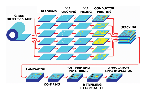
LTCC is a ceramic-based technology using low resistivity conductor material such as silver, copper or gold. Figure 1 shows the conventional process flow used to manufacture LTCC ceramic multi-layer substrates. With regard to integration of passive elements, LTCC offers the potential to build composite ceramic structures mixing low and high permittivity dielectrics as well as ferrite materials to enlarge its capabilities of capacitors and inductors.
Technical Approach
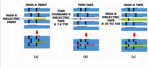
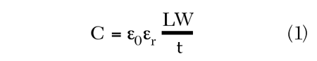
Several solutions are used to build integrated capacitors within an LTCC multi-layer substrate.1 The two most common approaches are shown in Figure 2. The first option consists of printing locally a high-k paste on the standard tape (a). In the second approach, the standard LTCC tape itself is used as the dielectric of the capacitor. With this technique, thinner tapes and several layers can be stacked to increase the capacitance density.5 Due to the poor thickness accuracy of the printing process, solution (a) is not suitable to build high tolerance capacitors and is therefore not relevant for filtering applications. Due to the better thickness control of the tape casting process, option (b) can offer better capacitance accuracy. However, the low dielectric constant of the standard LTCC materials (7.8 for DuPont 951) limits the capacitance density to 2 to 3.5pF/mm2/per layer depending on the tape thickness. The determination of the capacitance of a parallel capacitor is described in Equation 1.
edge effect excluded
rectangular electrodes
where

L = electrode length
W = electrode width
T = dielectric thickness
ε0 = permittivity of the dielectric material
To offer better density together with a satisfactory thickness control, a third alternative can be considered consisting in using a high-k dielectric tape (see Figure 2). Figure 3 compares the integration density of the high-k tape solution to the capability of the standard thin tape option. In the selected example, the capacitance density of the high-k layer is 15 pF/mm2 for a single layer. As shown by the graph the high-k tape allows reduction of the number of layers, leading to potential cost savings and/or reduction of the size of the capacitor bringing module size reduction. As an example, to design a 10 pF capacitor, the high-k tape requires an electrode size of 0.82 x 0.82 mm with a single layer while 0.91 x 0.91 mm and six layers or 1.1 x 1.1 mm and four layers are necessary using the standard tape material. However, this approach needs a specific material featuring good compatibility with the standard LTCC material. Evaluation of mixed-dielectric structures to build buried capacitors in LTCC have been reported,2-4 mentioning dielectric permittivity in the 20 to 150 range. So far, however, only a few high-k tape materials are commercially available from conventional LTCC material suppliers. It was decided to develop and study a new material suitable for high frequency applications featuring low dielectric losses (tanδ < 10–3), medium permittivity in the 80 to 100 range and limited dielectric constant drift over temperature (less than 250 ppm/°C).
Development of the New High-K Tape
The high-k dielectric composition Bi2Zn2/3Nb4/3O7 was chosen, as it presents the targeted properties: sintering temperature below 1000°C, dielectric constant about 90, with temperature coefficient about 150 ppm/°C, and dielectric loss tangent lower than 10–3 at 1 MHz.6–8 BZN dielectric materials were produced using the standard ceramic process, as previously described.9 The permittivity and dielectric losses of sintered material samples were measured using the dielectric resonator method. The following results were obtained:

• Permittivity: 77.8 at 2.9 GHz
• Dielectric losses: 1.10–3 at 2.6 GHz
• Thermal Coefficient: 230 ppm/°C at 1 kHz In order to use this dielectric composition in LTCC multi-layer, 100 μm thick BZN tapes were prepared through the Doctor-Blade technique. Different composition/casting experiments were performed to obtain the optimal mechanical properties of the tape.9
BZN/DP951 multi-layer stacks were studied for co-firing with the standard LTCC process in order to analyze the diffusion at material interfaces as well as the sintering density.
The results shows very good compatibility: the interface between materials is dense and smooth and a well-controlled diffusion zone between materials of about 2 microns thickness was observed through Scanning Electron Microscopy (SEM) and Energy Dispersive Spectroscopy (EDS) techniques.
LTCC Process Adaptation

Starting from the conventional LTCC process, all the manufacturing steps were adapted to the new material as well as the mixed dielectric structure. A particular emphasis was dedicated to the sintering operation to allow the realization of flat substrates with the so-called free sintering option. Regarding the shrinkage in x and y of the substrate after co-firing, it was demonstrated that 951/BZN sandwiches such as 2 x 951A2/1 x BZN/2 x 951A2 allow the nominal shrinkage of the 951 dielectric to be preserved (that is, 12.7 percent).
Test Vehicles Design and Realization
A specific test vehicle (TV2) was designed to perform the electrical characterization of the integrated capacitors. This test vehicle includes in total 42 capacitors featuring various electrode dimensions and configurations. Figure 4 shows the typical vertical structure of an integrated parallel capacitor designed with a single BZN layer. The top electrode width and length vary from 550 to 1650 μm while its resulting area varies from 0.30 to 1.8 mm2. The bottom electrode is 100 μm larger than the top one (50 μm on both sides) to reduce the effect of possible misalignment between electrodes on capacitance variation. To allow RF measurement, the top electrode of each buried capacitor is connected via a microstrip line to coplanar access pads printed on the top surface of the LTCC substrate. A set of RF calibration structures is also included in the test vehicle design.

Several panels of this specific test vehicle were manufactured for technology evaluation and RF characterization purpose. A picture of a test vehicle sample is given in Figure 5 showing its topside with the RF access pads.
The flatness of the test substrate was verified. The optimized sintering profile allows satisfactory results to be obtained, the overall camber being lower than 0.3 percent of the panel diagonal.
Several cross-sections of the test vehicle were realized to check the integrity of the multi-layer structure. The picture in Figure 6 shows a typical cross-section of an integrated capacitor. No voids or delamination occurs at the high-k BZN/951 interface. The average value of the high-k BZN dielectric thickness is 62 μm (between electrodes).
Building mixed dielectric multi-layer may degrade the mechanical performance. The flexural strength and the Young modulus of the substrate was therefore verified, performing three-point bending test on mixed structures as well as on pure 951 stacks. The two configurations did not show any significant difference giving average values of 250 MPa for flexural strength and 100 GPa for Young modulus.
RF Characterization

As previously mentioned, all the embedded capacitor test structures on test vehicles are connected to the top surface of the LTCC panel via the same interface made of a 50 Ω microstrip line terminated with a 50 Ω coplanar pad structure. Capacitor elements were measured from 50 MHz to 6 GHz with coplanar microwave probes (ground-signal-ground, 350 μm pitch, 40 GHz).
The vector network analyzer (VNA) was calibrated using the SOLT calibration kit included on the test panel, so the measurement reference plane is located at the edge of the top capacitor electrode. The S-parameters obtained from the VNA were processed via a microwave circuit simulation software.
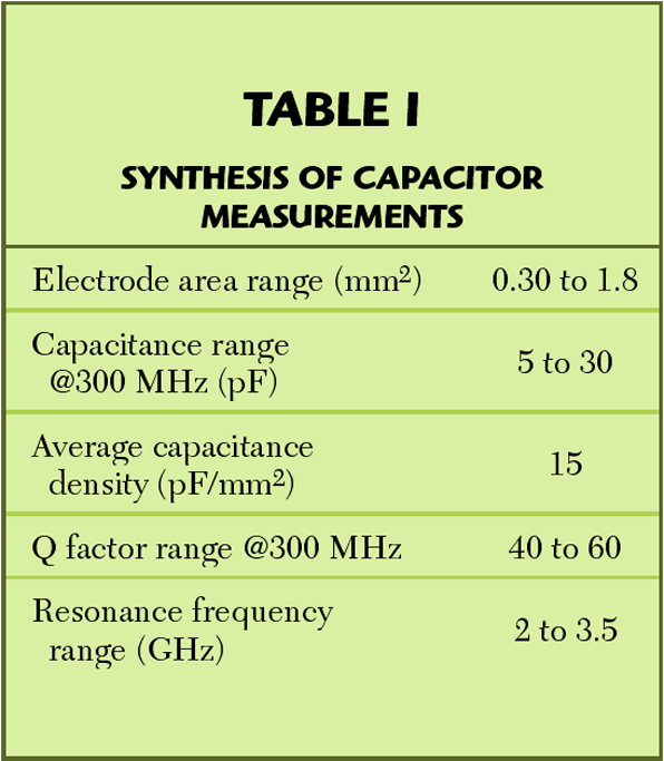
Figure 7 gives the typical result obtained on the smallest capacitor structure A0 (electrode area = 0.30 mm2). Considering the whole measured batch, the A0 structure gives the following average parameters:
• Capacitance at 300 MHz = 5.1 pF
• Quality factor at 300 MHz = 50
• First resonance frequency = 3.5 GHz The different capacitor test structures featuring various electrode sizes and shapes were measured on several LTCC test panels. Table 1 gives the synthesis of the overall results.
3-D Electromagnetic Simulations
The embedded capacitor was described (see Figure 8) and simulated with a 3-D Electromagnetic (EM) simulation software aiming to:
• Determine the parasitic elements and understand the influence of materials performance
• Optimize the design of the capacitor structure limiting the number of the time-consuming and costly test vehicle design-manufacture-test iterations
The 3-D EM simulation software used presented some mode confusions when the structure was simulated with grounded coplanar ports. In order to overcome this issue coplanar and microwave probes were included in the simulated structure, as shown in Figure 9. With this structure, the access port becomes coaxial and thus eliminates the mode confusion issue. To shift back the electrical reference plane to the capacitor element, the complete access structure was simulated as well to obtain the S2P parameter file. The S2P parameter file was then used to determine the de-embedded results with the microwave circuit simulator.

Thanks to this method, satisfactory simulation results were obtained giving good correlation between RF measurements and simulation, as shown in Figure 10.
Further simulation experiments allowed some routes to optimize the Q factor to be identified. In particular, it was demonstrated that additional grounding via-holes increased the Q factor significantly.
Electrical Modeling
An electrical model of the A0 capacitor structure was designed (see Figure 11). In this model, the low frequency (before the first resonance) behavior is mainly modeled by the elements TL1, R3 and C1. The high frequency behavior (from the first resonance) is mainly modeled by the two resonant circuits SRLC1 and PRLC1.
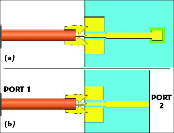
Figure 12 shows the correlation between the response of the electrical models and the RF measurement. In the same way this model can be fitted to different capacitor dimensions in order to design a parameterized model. Such a model, implemented on a microwave circuit simulator, allows one to perform the simulation and optimization of filter structures easier and faster.
Assembly and Environmental Evaluation
The compatibility of the developed material and process with assembly and packaging techniques was evaluated by performing wire-bonding trials and flip chip assembly experiments as well as building BGA structures. A second test vehicle was designed for this purpose and two batches were manufactured: a first one with the high-k BZN layer and a second one without the high-k BZN layer as the reference (conventional LTCC). All the assembly trials performed did not point out any drawback related to the high-k BZN technology with regard to the different process aspects. As an example, Figure 13 shows a cross-section of a flip chip assembly structure on a high-k BZN/DP951 test panel.
To evaluate the reliability of the developed integrated capacitor technology, several TV2 test panels were submitted to extensive environmental trials. Three groups were defined to go through the following tests:

• High temperature storage: 1000 hours @ 150°C
• Damp heat test: 1000 hours @ 85°C, 85% RH
• Thermal shocks (2-chamber test): 500 cycles –55°C/+125°C Each capacitor was measured before and after environmental tests as well as at intermediate steps. No failure occurred and no significant drift of the capacitance values was observed along the different tests.
Conclusion
A new high-k tape was developed to allow the integration of filtering capacitors in an LTCC substrate. This material is well adapted to the DuPont 951 base material system and inner silver conductors. Providing some specific process adaptations it is fully compatible with the conventional LTCC manufacturing flow and does not affect the assembly and packaging capabilities of the standard technology. In addition, good reliability of the mixed-dielectric structures was demonstrated through high temperature storage and a damp heat test as well as thermal shocks. The new material provides a nominal capacitance density of 15 pF/mm2 with a single layer compared to 2 pF/mm2 with the standard LTCC tape. Capacitor test structures from 4 to 30 pF were produced and characterized in the 300 MHz to 10 GHz frequency range showing satisfactory properties for use in RF applications up to 2 GHz. Finally, adapted electrical simulation models were defined providing a satisfactory agreement with the RF measurements.

Acknowledgments
The presented RTD activities were performed in the frame of the PIDEA PACIFIC BOAT project (EUREKA mainframe) and the Fanimat nano shape project. The authors would like to thank the PIDEA organization, the Direction Générale des Entreprises (French Ministry of Industry), the German Ministry of Education and Research (BMBF), and the Projektträger Jülich organization for their support.
References
1. J. Müller and D. Josip, “Integrated Capacitors Using LTCC,” MicroTech 2002, January 29–30, 2002, Manchester, UK.
2. T. Bartnitzek, E. Müller and R. van Dijk, “LTCC Phase Shifter Modules for RF-MEMS Switch Integration,” IMAPS CICMT, April 10–13, 2005, Baltimore, MD.
3. M. Lahti, K. Kautio, E. Juntunen and P. Karioja, “High Power Module Integrated in LTCC Package,” 3rd EMRS DTC Technical Conference, Edinburgh, Scotland, 2006.

4. V. Sunappan, P.L. Vadiveloo, L.L. Wai, W. Fan and C.W. Lu, “Processing and Electrical Characterization of Co-sintered Composite Glass Ceramics,” 2006 Electronics Packaging Technology Conference.
5. J.P. Cazenave, J. Cerisier, S.K. Choi, L. Boyer, P. Henquenet, J. Cocker, C. Pickering, C. Wang, M. Barker and C. RS Needes, “Improved RF Circuit Performance with an Enhanced and Expanded LTCC System,” 14th European Microelectronics and Packaging Conference & Exhibition, Friedrishshafen, Germany, 23–25 June 2003.
6. D.H. Liu, Y. Liu, S.Q. Huang and X. Yao, “Phase Structure and Dielectric Properties of Bi2O3-ZnO-Nb2O5-based Dielectric Ceramics,” J. Am. Ceram. Society, 76 [8] 2129-32 (1993).
7. X.L. Wang, H. Wang and X. Yao, “Structures, Phase Transformations and Dielectric Properties of Pyrochlores Containing Bismuth,” J. Am. Ceram. Society, 80 [10] 2745-48 (1997).

8. M.F. Yan, H.C. Ling and W.W. Rhodes, “Low Firing, Temperature-stable Dielectric Compositions Based on Bismuth Nickel Zinc Niobates,” J. Am. Ceram. Society, 73 [4] 1106-107 (1990).
9. J.P. Ganne, M. Paté, R. Lebourgeois, J.P. Bertinet, E. Leleux, E. Mueller and F. Bechtold, “Filtering Capacitor Embedded in LTCC Substrate,” IMAPS ATW on Passive Integration, November 11–15, 2007, San Jose, CA.