
The use of discontinuities in ground planes or in microstrip lines is currently employed to improve the performance of different passive circuits, such as the size reduction of amplifiers,1 the enhancement of filter characteristics2,3 and applications to suppress harmonics in patch antennas.4 On the other hand, a new proposal, called defected microstrip structure (DMS), has been successfully used in reducing the size of, and as a tuning technique for, rectangular patch antennas.5,6 The DMS is similar to the structure called spurline,9 since both are etched in the microstrip line and behave as stop-band filters. The main difference, however, is that DMS achieves a greater associated inductance. DMS also presents a greater slow-wave effect, since it has more discontinuities, providing a longer trajectory to the electromagnetic wave. Simultaneously, DMS also performs a greater stop-band bandwidth compared to spurline, both having the same dimensions.
In a previous article,5 the reduction of the antenna size, resonating at 1.77 GHz, was made by iterations with simulation software, just assuming a reactive load introduced by the DMS. That procedure is highly time-consuming compared to the method developed in this work and the antenna dimensions can be predicted perfectly with great accuracy. In another article,6 the DMS was employed as a tuning technique for rectangular microstrip antennas, as an alternative procedure for lowering the resonance frequency in which a mathematical model was proposed to obtain the associated inductance introduced to the radiator with the defect. A 1.45 GHz antenna was designed and tuned by using that method.

In this article, a square patch antenna resonating at 3 GHz and a matching network with an open-circuited stub are developed to demonstrate the efficiency of the simplified method for reducing dimensions and the size reduction is predicted. Furthermore, such methods can be generalized in almost all microstrip circuits. The use of DMS or DGS consequently allows an increase in the slow-wave factor (SWF) in transmission lines in which they are introduced. This phenomenon can be used to reduce the size of passive planar circuits like microstrip line lengths, coupling lines and microstrip antennas, among other microstrip structures. However, no mathematical method has been explained so far to apply this phenomenon in such circuits. In the present work, a very simple and accurate method to describe how defected structures can be used in reducing the size of microstrip structures and predict their new dimensions is developed.
Slow-wave Factor in Microstrip Lines with Defected Structures
The SWF is the relationship between the wave number in free space, k0, and the propagation constant, β, of the transmission line. For loss less microstrip line, the SWF is determined by

where εe is the effective permittivity of the material, and the propagation constant is determined by

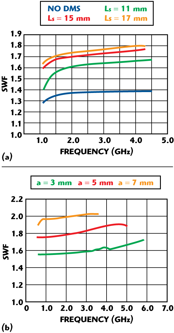
The SWF of a microstrip line is raised when a discontinuity is introduced in the path of the electromagnetic wave, increasing the impedance of the line.7 There are many works specifying diverse types of discontinuities applied in microstrip lines, including photonic band gap structures (PBG). Two of these structures are show in Figure 1.
To show the behavior of the SWF in a microstrip line with a physical length l and an electric length θ, a 50 Ω microstrip line is designed using a substrate material with a dielectric constant of 2.2 and 1.27 mm thick. The line width is 4 mm and its physical length is 22 mm. The electrical length of this line is obtained by means of electromagnetic simulation (EM). A DGS unit-cell is subsequently introduced under the line and the cell dimensions are varied from a smaller to a larger size and the new microstrip line electrical length for those values is obtained. Finally, the SWF of the total structure is obtained. A similar procedure is used when a DMS unit-cell is introduced. The results are shown in Figure 2. It is clear that both structures increase the SWF in the microstrip line, showing a greater increment with the DGS structure for a smaller unit-cell dimension. In spite of the apparent advantage of the DGS unit-cell, however, the DMS structure could be the unique solution for certain applications, particularly due to its geometric properties.
Method to Reduce Dimensions of Microstrip Circuits
Most applications of DGS and DMS structures have been successfully achieved purely by simulation. The method proposed in this work establishes a very simple and accurate procedure to find the new and reduced dimensions of conventional lines when a defect is introduced in the microstrip structure. These applications include filters, stubs and patch antennas among other microstrip circuits. To achieve the method, it is necessary to find the electrical length introduced in a microstrip line when a DGS or DMS unit-cell (or several unit-cells) are employed. Every circuit based on transmission lines presents an electrical length, and for microstrip lines the electrical length is given by

Strictly speaking, microstrip circuits can be separated as cascaded black boxes and their respective electrical length calculated. On the other hand, these lines show a resonant frequency, fr, by themselves. In many cases, lines can be seen as resonators, and in this case, for simplicity, a λg/4 line resonator is considered, where λg is the wavelength in the material, either in an open- or short-circuited configuration. In the case of microstrip lines, fr is given by

where
l = physical length of the line
c = speed of light in free space
For each line, the respective resonant frequency must be found and, at that frequency, the wave number in free space, k0, is obtained. The next step is to propose a unit-cell dimension (or a pattern of unit cells). The structure can be either a DGS or DMS, and this is introduced in the microstrip line and for such a configuration, the electrical length, θc, at fr is obtained by EM simulation. From these results, the SWF is

After introducing the unit-cell in the microstrip line, the substrate employed in the implementation presents an apparent effective dielectric constant, εec, which is larger than the real effective dielectric constant εe. This apparent permittivity provides the tool to explain how the dimensions of microstrip circuits can be reduced, which means that for a higher dielectric constant the wavelength is shorter as well as the microstrip circuits, both being a function of this parameter. Since the original microstrip lines have an electrical length and introducing a DMS/DGS unit-cell into the structure increases it, a new dimension must be found to keep the electrical length equal to that of the non-defected lines. The new length that gives the original electrical length for the microstrip line with DMS/DGS unit-cell is obtained from

Simulation and Experimental Results
To exemplify the proposed method, two microstrip circuits were designed: a matching network with an open-circuited stub to match a load of 200+j100 Ω to a 50 Ω line at 2 GHz, and a rectangular patch antenna resonating at 3 GHz.
Matching Network
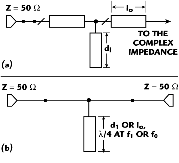
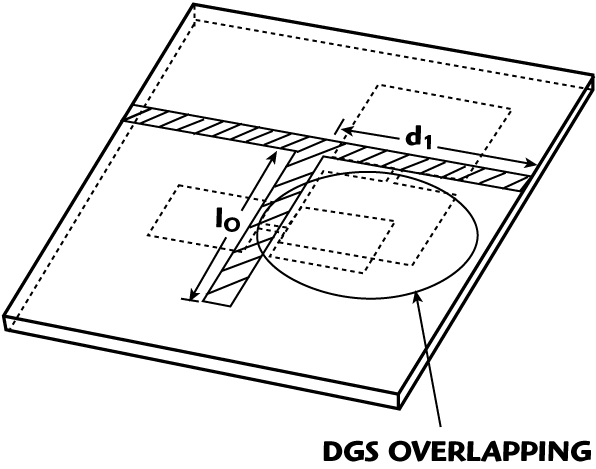
Considering the conditions previously mentioned, the matching network with an open-circuited stub has the dimensions d1 = 22.98 mm and lo = 29.73 mm, where d1 is the line length from the complex load to the stub and lo is the stub length. Both lines have, independently, electrical lengths θd and θ1. Configured as a λ/4 line resonator, as depicted in Figure 3, they present resonant frequencies fd and f1, respectively.
The matching network is also displayed in the figure. The resonant frequency for each line is fd = 2.36 GHz and f1 = 1.83 GHz; the wave number at those frequencies is k0d = 49.42 m–1 and k01 = 38.32 m–1, respectively. Following the procedure explained in the slow-wave factor in microwave lines with defected structures section, a DGS unit-cell is proposed to achieve a larger SWF, and therefore increase the electrical length and reduce the physical length of the lines. After some iterations in the procedure, a DGS unit-cell with a =7.5 mm is suggested for being used under the microstrip line with length d1. By using EM simulation, the electrical length of the line with the DGS cell at 2.36 GHz is 145.88°. From Equation 5, SWF = 2.24; from Equation 6, the new dimension of the microstrip line with the DGS unit-cell is obtained, which is d1c = 14.17 mm.
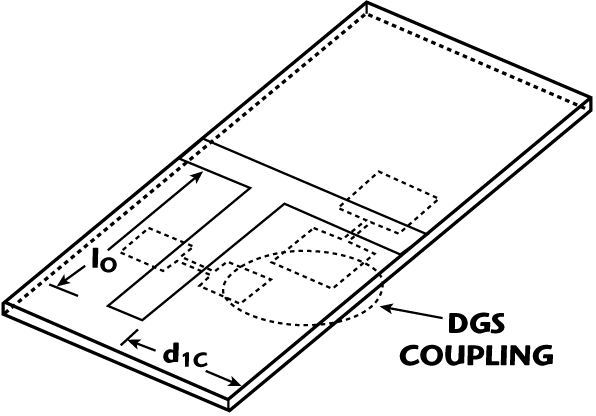
In the case of the microstrip with length lo, another even larger DGS unit-cell could also be proposed since lo > d1, so the length can be diminished in a greater proportion. Following the same procedure, a 5 mm DGS unit-cell is proposed, obtaining a reduced dimension of lo = 23.5 mm. The structure with two DGS unit-cells is shown in Figure 4.
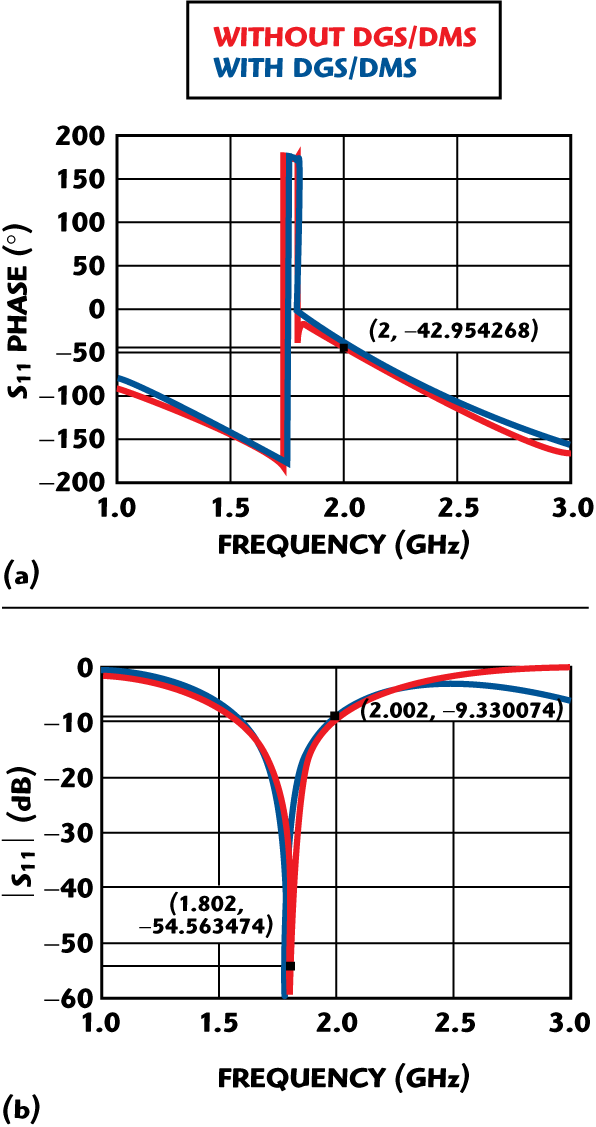
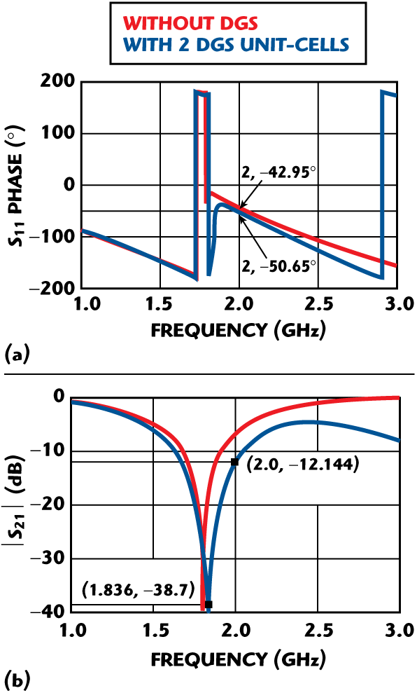
To analyze the performance and behavior of the matching network with the open-circuited stub with and without imperfections, the structures are analyzed as two-port black boxes. The results are shown in Figure 5, where a comparison with the conventional stub can be observed. It is shown that the response of the open-circuited stub is not adequate, since there is a difference of 8° in the phase response, and more than 7 dB in the magnitude response in comparison with the conventional stub.
This divergence in the response is due to the fact that there is an interaction between the unit-cells because of their proximity in the ground plane, which gives rise to a coupling between the structures. The associated inductance of each one is modified, resulting in a different electrical length for the lines. Therefore, the use of two DGS unit-cells in this kind of structure would not be the most viable solution, since there could be a worst case: a cell overlapping, as shown in Figure 6. Because of the problem described, the use of a DMS unit-cell instead of a DGS cell is proposed to reduce the length of the second line. This way there is no interference in the performance of each imperfection, now that one is located in the ground plane under the microstrip line with a length d1 and the other is placed over the second microstrip line.
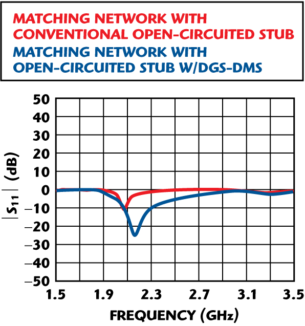
After some iterations and analyses of the behaviour of the electric length, and in order to achieve a large reduction of dimensions, the unit-cell obtained is 15 mm long by 2 mm wide. The line with the DMS cell is simulated and the electrical length of the complete structure is obtained. This electrical length is 111.66° at 1.83 GHz. Using Equations 5 and 6, the SWF is 1.71 and the new reduced length is l0c = 23.9 mm. The total reduction of both lines is 36 and 20 percent for d1 and lo, respectively. The results from simulation of the open-circuited stub with no defects and the structure with DGS and DMS unit-cells are shown in Figure 7, in which a great convergence is observed, especially at 2 GHz, where the circuit was designed to operate.

Figure 8 is a photograph of the matching network with DSG and DSM unit-cells. The measured S11 response of both structures is shown in Figure 9, showing similar performance at the design frequency and a better behaviour in the case of using an open-circuited stub with DGS/DMS unit-cells to implement the matching network, considering bandwidth and matching.
Square Patch Antenna
A microstrip rectangular patch antenna is an element that can be seen as a λ/2 line resonator. The dimensions of such a structure are L x W, where L is the element length and W is the element width, as shown in Figure 10. To apply the size reduction method to these kinds of structures, a procedure similar to the one previously explained is followed.
A conventional antenna is designed to resonate at 3 GHz and its performance is analyzed. The substrate material on which the antenna is built has a dielectric constant of 2.2 and a thickness of 1.27 mm. The calculated dimensions of the antenna are L = 33 mm and W = 39.5 mm and the feeding line is 4 mm wide. The antenna has a physical structure derived from a microstrip transmission line.8 The patch antenna is modeled as a length of transmission line of characteristic impedance Z0 and with a propagation constant γ = α + jβ. The fields vary along the length of the patch and remain constant across the width. Then, to simplify the analysis, the antenna can be seen as a microstrip line with length L and the width can be modified to handle a smaller magnitude. Therefore, a thinner element can be used.
A line width of W1 = 4 mm is proposed, considering the substrate’s characteristics necessary to obtain a 50 Ω impedance, to facilitate the simulation procedure. With this line of length L = 33 mm and W1 = 4 mm, by using Equation 4, the resonant frequency is obtained when the element is working as an open-circuited λ/4 resonator, fr = 1.66 GHz and the wave number at this frequency is k0 = 34.76m–1. To optimize the size reduction of the antenna, it is necessary to provide the largest possible SWF without degrading the performance of the device for which a large enough DMS unit-cell is proposed. The dimensions of such a cell are 20 mm long by 2 mm wide. In the next step, the electrical length of the structure with the unit-cell at fr is obtained by EM simulation. In this case, θc = 113.5° at 1.66 GHz.
By using Equations 5 and 6, the new length of the antenna with the DMS unit-cell is Lc = 25.9 mm. The ratio W/L is kept to maintain the cross-polarization levels sufficiently low; therefore, the new dimension of W is Wc = 30 mm, obtaining an area reduction close to 40 percent. The simulated reflection coefficient and gain of the conventional rectangular patch antenna and the reduced patch antenna with DMS unit-cell are displayed in Figures 11 and 12.
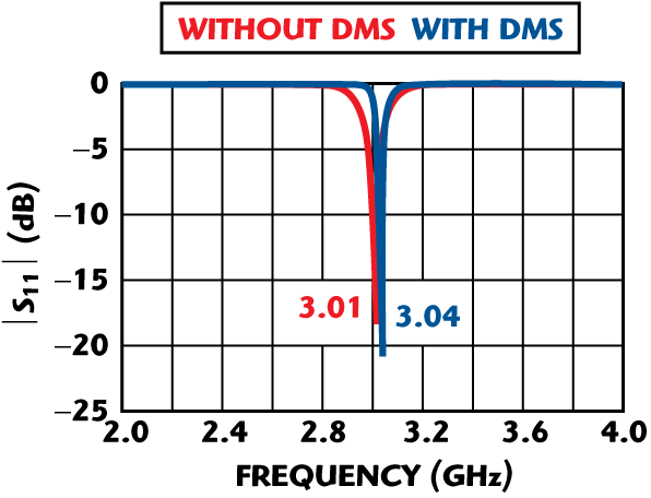
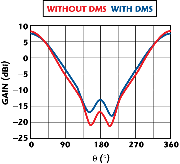
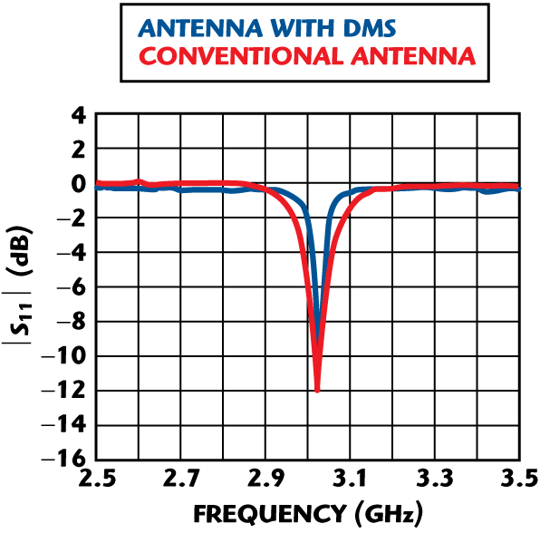
A good agreement is observed between the conventional and the reduced patch antenna, concerning matching and resonance. The difference between these two curves is very small, and a tuning technique can be employed to move the resonance of the patch antenna with DMS from 3.04 to 3.00 GHz. On the other hand, the gain and radiation pattern in both antennas remains almost the same. Consequently, introducing DMS slots in the non-radiating edges does not considerably modify the characteristics of these antennas. The measured resonant frequency of both antennas is shown in Figure 13. These results are similar to those obtained by EM simulation. It is then clear that the method employed to determine the new reduced length and dimensions of a rectangular patch antenna is effective and accurate. The difference between the dimensions of unit-cells and line lengths obtained by formulas and by simulation for adequate performance is close to three percent in both microstrip circuits, which is a good trade-off.

Conclusion
In this work, a simplified method to foretell the reduced dimensions of microstrip circuits is proposed. The procedure is based on simple formulas, and EM simulation to obtain the SWF is introduced, when DGS or DMS cells are employed in passive planar circuits. The method is based on the reduction of the phase velocity in lines with discontinuities, which means increasing the SWF. Generally, this can be applied to most microstrip circuits and is also useful when one or more DGS/DMS unit-cells are used to increase the SWF. The limitation of this method is the geometry of the microstrip circuit itself, when defected structures cannot be employed. By using this procedure, the size reduction of a matching network with an open-circuited stub was successfully achieved, improving the performance of the circuit in which a wider coupled bandwidth was observed and a size reduction of 20 to 36 percent was achieved. The size of a square patch antenna was also reduced, obtaining great results without modifying the behaviour of the original structure, concerning resonance frequency, coupling, gain and radiation pattern, and achieving an area reduction close to 40 percent. The predicted size reduction differs by approximately three percent from the experimental one.
Acknowledgment
This work was supported by CONACyT-SEMAR project 2003-C03-11873, Mexico.
References
1. J.S. Lim, Y.T. Lee, C.S. Kim, D. Ahn and S. Nam, “A Vertically Periodic Defected Ground Structure and Its Application in Reducing the Size of Microwave Circuits,” IEEE Microwave and Wireless Components Letters, Vol. 12, No. 12, December 2002, pp. 479–481.
2. J.S. Lim, C.S. Kim, Y.T. Lee, D. Ahn and S. Nam, “Design of Low Pass Filters Using Defected Ground Structure and Compensated Microstrip Line,” IEE Electronics Letters, Vol. 38, No. 22, 24 October 2002, pp. 1357–1358.
3. J.S. Lim, C.S. Kim, D. Ahn, Y.C. Jeong and S. Nam, “Design of Low Pass Filters Using Defected Ground Structure,” IEEE Transactions on Microwave Theory and Techniques, Vol. 53, No. 8, August 2005, pp. 2539–2545.
4. H. Liu, Z. Li, X. Sun and J. Mao, “Harmonic Suppression with Photonic Bandgap and Defected Structure for Microstrip Patch Antenna,” IEEE Microwave and Wireless Components Letters, Vol. 15, No. 2, February 2005, pp. 55–56.
5. J.A. Tirado-Mendez, H. Jardon-Aguilar, F. Iturbide-Sanchez, I. Garcia-Ruiz, V. Molina-Lopez and R. Acevo-Herrera, “A Proposed Defected Microstrip Structure (DMS) Behavior for Reducing Rectangular Patch Antenna Size,” Microwave and Optical Technology Letters, Vol. 43, No. 6, December 2004, pp. 481-484.
6. J.A. Tirado-Mendez, H. Jardon-Aguilar and F. Iturbide-Sanchez, “Application of the Defected Microstrip Structure as a Tuning Technique for Rectangular Printed Antennas,” Microwave and Optical Technology Letters, Vol. 48, No. 2, February 2006, pp. 370–373.
7. J.S. Lim, C.S. Kim, Y.T. Lee, D. Ahn and S. Nam, “A Spiral-shaped Defected Ground Structure for Coplanar Waveguide,” IEEE Microwave and Wireless Components Letters, Vol. 12, No. 9, September 2002, pp. 330–332.
8. G. Ramesh, P. Bhartia, I. Bahl and A. Ittipiboon, Microstrip Antenna Design Handbook, Artech House Inc., Norwood, MA, 2001.
9. E.G. Cristal, “Bandpass Spurline Resonators,” IEEE Transactions on Microwave Theory and Techniques, Vol. 14, No. 9, September 1966, pp. 436–436.
 José Alfredo Tirado-Méndez received his BS degree in electronics and digital systems from UAM-Azcapotzalco and his MSc degree in telecommunications from CINVESTAV in 1999 and 2001, respectively. He joined the Microwave and Remote Sensing Laboratory at the University of Massachusetts in 2001. In 2002, he joined the Telecommunications Section at CINVESTAV as a research assistant. He is currently working toward his PhD degree in telecommunications at CINVESTAV-Mexico. His research interests include electromagnetic compatibility and nonlinearities as well as RF and microwave circuit design, patch antennas and microstrip filters.
 Hildeberto Jardón-Aguilar received his BS degree in electrical engineering from ESIME-IPN and his PhD degree in radio systems from the Moscow Technical University of Telecommunications and Informatics. He has been working at the Center of Research and Advanced Studies since 1985 and is currently a full professor. His research interests include analysis of nonlinearities in RF and microwave circuits, electromagnetic compatibility and photonic systems.
 Edgar Alejandro Andrade-González received his BSEE degree from Autonomous Metropolitan University (UAM), Mexico, in 1994. He is currently working toward his master’s degree in electrical engineering at CINVESTAV-IPN. He is a professor in the department of electronics and communications at Metropolitan Autonomous University-Azcapotzalco. His research interests include personal communications and the design of electronic circuits for high frequencies.
 Mario Reyes-Ayala received his BSEE degree from Metropolitan Autonomous University (UAM), Mexico, in 1994, and his MSEE degree from CINVESTAV-IPN, Mexico, in 2005. From 1994 to 1996, he was a department head at AEG Mexicana in Mexico City. In 1999, he joined the electronic department at UAM and he has been engaged in studies on digital satellite communications and propagation models for radio communication systems. His research interests also include theoretical analysis in satellite interference phenomena.