
In the 28 years that I have been both a user and designer of solid-state switches, I have witnessed some major technological advances as RF switches have developed from discrete PIN diodes and evolved through recent developments such as HMIC, GaAs MMICs and RF CMOS. Significantly, too, new technologies on the horizon have the potential to impact on the long-term development of RF switches and take them to a new level.
Discrete PIN Diode Switches
How have solid-state switches evolved? My first professional involvement with them came in the mid-1980s when, as a young engineer, I was tasked with designing one of Filtronic’s first subsystem products. The design required 2 to 18 GHz high-speed switches and attenuators, and as I had no experience in the design of switches at that time, I selected a well-established supplier who also had a PIN diode fabrication facility.
The prototype parts arrived, were tested and a number of issues identified. Consequently, I visited the supplier to review the design and identify corrective actions. During the review it was suggested that in order to obtain the required performance, the suppliers could select a different diode ‘lot’ and I found myself in a room reminiscent of a Victorian apothecary containing wafers of diodes of almost every possible variety.

Not quite Victorian, but a product of the 1950s, the basic PIN diode is a standard PN junction diode with a thin layer of intrinsic material, with a very low level of doping, introduced between the P and N regions. This has the effect of isolating the active regions under low reverse bias conditions as the I-region is fully depleted. When the diode is forward biased, charges are injected into the intrinsic region allowing current to flow across the layer.
The electrical characteristics of the diode such as junction capacitance, breakdown voltage and minority carrier lifetime can be altered by changing the process parameters, such as I-thickness, doping levels and electrode dimensions. In addition, exotic ingredients like gold can be added to achieve ‘special’ characteristics. To form a high isolation RF switch, the PIN diodes are arranged in a series/shunt configuration.
The chip shunt diodes (see Figure 1) are mounted on the ground plane, which provides both the electrical connection for the cathode and a thermal path to remove heat generated from the bias current and any RF heating under high power conditions. The shunt diodes are connected using thermo-compression bonding and the gold wire bond inductance can be conveniently designed to match the junction capacitance to form a low pass structure. The series diodes are more of a problem as lead inductance and junction capacitance severely limit the achievable isolation, so a ‘beam-lead’ diode is used. This is a silicon die encapsulated in glass to which thin gold ‘beams’ are attached and connected to the active regions (see Figure 2). The beam-lead diode gives a dramatically improved performance and together with the shunt chip has been the mainstay of broadband RF switches for decades.

Although the discrete PIN diodes perform well, the manufacturing costs are high and they are prone to assembly variations resulting in degradations of the VSWR and loss. Figure 3 shows a typical 2 to 18 GHz high isolation PIN switch, with a close up of the common junction highlighting the intricate connections of the series and shunt diodes.
Monolithic PIN Diode Switches
Monolithic technology made significant inroads in the 70s and 80s, but had little impact on the design of microwave switches as the silicon substrate used for PIN diodes is highly conductive and is unsuitable for fabricating the interconnects and series diodes required. However, in the late 1980s, the M/A-COM corporate R&D team pioneered the use of the Glass Microwave Integrated Circuit (GMIC).

This was an alternative to the conventional GaAs MMIC and fused an active GaAs wafer with a glass substrate, which allowed active devices to be realised together with very low loss passive elements and with vias introduced through the glass substrate to provide electrical grounding. A variant of this technology continues today as M/A-COM’s patented Heterolithic Microwave Integrated Circuit (HMIC) technology. Here, a glass substrate is fused to a silicon wafer, and the silicon wafer is etched to create silicon pedestals. A glass layer is deposited on and around the silicon pedestals and polished to expose the mesas. Conductors and air bridges are added and backside vias are etched though the glass substrate and plated to connect to the underside of the silicon.
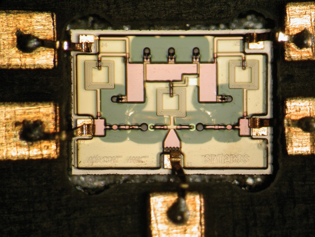
HMIC technology has enabled complete multipole series shunt switches to be manufactured and eliminated the very difficult connection of the beam-lead diodes and the first shunt diode that had long plagued designers. Some designs, such as MA4SW210B-1, also include the bias circuitry, significantly simplifying the manufacturing process and the reproducibility, as shown in Figure 4. However, it may still be necessary to use a more distributed approach if more than 50 dB isolation is required, with additional shunt-only HMIC parts separated by lengths of transmission lines.
GaAs PIN Switches
A further enhancement of the PIN technology saw the introduction of PIN diodes on GaAs substrates. TriQuint Semiconductor offers a vertical PIN (VPIN) foundry process, which achieves lower capacitance than silicon devices and allows operation beyond 50 GHz. The VPIN process allows MMIC switch integration, but cannot be mixed with active devices. M/A-COM recently combined a patent-pending anode-enhanced AlGaAs PIN diode with the HMIC process to produce a range of high performance multi-throw switches such as the SP3T MA4AGSW3, which provides 0.8 dB loss with greater than 30 dB isolation at 50 GHz (see Figure 5).
The range of HMIC switches can be used to replace the majority of legacy discrete PIN diode designs and offers reduced manufacturing cost and significantly enhanced reliability. These parts are very easy to use and offer the designer a very fast and reliable approach to switch design that I could only have dreamed about 10 years ago. Furthermore, the bespoken discrete PIN design has been replaced by a process-based, off-the-shelf part, in a similar way to the evolution from transistors to ICs. The only limitation is that there is only a restricted range of processes, and hence of diode parameters available, so there is still a place for handcrafted designs, which can in some cases offer better performance for very specific applications. Limiters are a prime example.

GaAs FET Switches
Although PIN diode switches have advanced enormously, they still require a DC bias current to achieve the low loss state and a high reverse voltage to achieve isolation. Biasing PIN diodes is notoriously difficult, as the bias must be applied to the RF signal path. This can result in reduced bandwidth and increased losses. In addition, high-speed switches generate large video transients that can adversely affect the circuitry to which they are connected. Also, high-speed PIN drivers are generally realised as thin film hybrids, which tend to be large and expensive.
An alternative switch element has long been available in the form of the field effect transistor (FET), where a voltage applied to the gate can alter the depletion region between source and drain to control the current flow. FETs have the advantage that the control voltage is essentially isolated from the main signal path and very low current is required (in the order of microamps). FET switches are widely used in various forms for low and high current switching at both video and RF frequencies. At microwave frequencies, the GaAs MESFET and more recently GaAs PHEMT devices have been used to replace PIN diode switches, particularly where very high switching speeds are required. GaAs FETs have inherently low charge storage and the channel itself can be switched in picoseconds.

Complete switches can be readily realised as MMICs and the bias control is very straightforward, without the need for bias chokes. When Filtronic set up a six-inch GaAs PHEMT foundry in 2000, I was a member of the Global Technology Group that had the opportunity to design MMIC components into the foundry in support of the process development team. I experimented with digital switched attenuators, analogue attenuators and distributed amplifiers, and was amazed at the scope that the process offered. By accurate characterisation and modelling, it was practical to get designs working the first time without needing any ‘tuning’ (something that had been almost impossible with the discrete designs I had been used to).
With the advent of low cost material and such high yield in six-inch foundries, these GaAs switches (see Figure 6) have become more widespread. They are available from a wide range of foundries and fab-less companies, such as Hittite and Mimix Broadband, who offer a range of similar products. An example of a broadband GaAs switch is the Filtronic FMS2030, an SP4T switch that exhibits more than 45 dB isolation and less than 1.5 dB loss at 20 GHz.
GaAs switches are ideal for use in complex switched filter assemblies, where the combined bias current of PIN diodes can be a significant issue and the simplicity of the bias networks is a major benefit to manufacturing costs. Level shifters are generally needed to interface to standard positive logic and are readily available as monolithic ICs. In some cases the drivers may be incorporated within the final packaged part. Compression points of +25 dBm are typical for broadband GaAs MMIC switches, which is somewhat lower than a typical PIN diode switch. However, they have the benefit of very low video leakage. GaAs MMIC switches lend themselves well to high levels of integration in the form of switched attenuators and phase shifters and can be easily integrated along with PHEMT amplifiers to produce complete RF modules.
Mobile Wireless Applications

Right through to the mid-1990s, PIN diodes remained the preferred option in early single- and dual-band mobile phones, due to their low cost. A circuit configuration was employed that resulted in the PIN diodes, requiring only to be forward biased during transmit, where the bias current was not a serious issue. However, this ‘trick’ could not be used when triple- and quad-band designs were introduced and GaAs PHEMT switches became the ideal choice.
The design of these switches is very demanding; positive only control is required with control voltages less than 2.5 V, transmit powers are in excess of 2 W and harmonic levels must be maintained below –70 dBc. Die size is also critical as the switches are very price sensitive. In 2003, I became involved in the design of handset antenna switches and we produced our first SP6T quad-band design. This was an exciting project and the design incorporated a novel topology to reduce the loss.1 This device is under 1 mm2 and is in use in a number of high volume phones (see Figure 7).
The introduction of 3G handsets now requires antenna switches to operate with a greatly increased level of linearity, with IMD3 levels of less than –110 dBm. This level of linearity requires a very accurate large-signal modelling, low parameter spread and a high yield, all of which have been successfully achieved with the Filtronic 0.5 μm GaAs PHEMT process. GaAs switches have been phenomenally successful and currently account for more than 50 percent of the available market. PIN diode switches are still used in relatively high volumes in the single- and dual-band phones aimed at the Far East market.
CMOS Switches
A recent challenger to GaAs for wireless applications has come in the form of RF CMOS. Historically, CMOS had been restricted to low frequencies due to limitations of the conductive silicon substrate. This has now been overcome by isolating the active devices from the base silicon substrate or using a low loss base substrate.

California Eastern Labs (CEL) uses a silicon-on-insulator (SOI) technology and offers an SPDT switch (UPD5710TK), operating to 2.5 GHz. Also, Peregrine Semiconductor has developed Ultra Silicon (UTSi®). This silicon-on-sapphire process was first invented in the early 1960s at Rockwell, but until recently suffered from poor yields and was not exploited. Peregrine has released a wide range of wireless products at frequencies up to approximately 5 GHz. One of its latest is the PE42693, an SP9T for mobile handsets (see Figure 8).
The major benefit of RF CMOS technology is the ability to integrate standard CMOS components like charge pumps and decoders. In addition, they can operate from single positive supplies and do not need DC blocking capacitors. CMOS is yet to gain a significant market share over GaAs, which is largely due to the low cost of six-inch GaAs fabrication and the immaturity of the RF CMOS process. This technology is likely to be a strong player in the future, however, although it is not yet clear how CMOS will compete at higher microwave frequencies.
Future Switch Technologies
Recent advances have been aimed at low power applications and PIN diodes are still the dominant force at very high powers, but there are a number of emerging technologies that may provide an alternative. Gallium nitride (GaN) on silicon carbide substrates has begun to take a share in the high power amplifier market with its ability to operate at voltages of greater than 100 V and at high temperatures. GaN switches have yet to appear on the market in great numbers but some research2 has been published, indicating that it can be used to construct very capable switches.
Mahamed Kameche3 gives an excellent review of the technology and concluded that GaN has a bright future for low distortion, high power switches, due to its high breakdown voltage, high saturated velocity and high thermal conductivity. It is currently only available on two- to three-inch wafers and as such is relatively expensive, although this should improve as volumes increase. The aerospace industry has long been looking for a technology that could be used to switch kilowatt levels at tens of amperes and at extremely high temperatures. The missile and radar industry would love to have devices to control kilowatts of power with very low losses and diamond may meet this challenge.
As an intrinsic material, diamond demonstrates extreme hardness, chemical inertness, high thermal conductivity, high hole and electron mobility, high dielectric strength and high breakdown strength, and has a wide band gap. These properties are ideal for high power amplifiers and switches. The recent availability of extremely pure single crystal diamond created by chemical vapour deposition has made it possible to contemplate the formation of diamond semiconductors. Diamond FETs are under development in the UK by Diamond Microwave Devices Ltd. (DMD), a subsidiary of Element Six Ltd., in collaboration with Filtronic plc. Diamond bipolar transistors are also under development at University College London under an Engineering and Physical Sciences Research Council (EPSRC) grant. Diamond technology is still in an early R&D phase, but the technology has the potential to make a major impact in the future.
Conclusion
RF switches continue to be a key component in all microwave systems. The expansion of the commercial wireless sector has had the effect of driving the costs down and has provided an impetus to develop technologies such as HMIC, GaAs and RF CMOS, together with low cost packaging systems. Coupled with a requirement for higher frequencies for WLAN, WiMAX and automotive radar, this technology has created exciting new products, most of which are readily utilised in the military and security sectors. There are a number of exciting technologies under development, including GaN and diamond that may allow solid-state switches to operate under very adverse conditions, where only mechanical switches have so far been practical.
References
1. D. Gotch, T. Goh and R. Jackson, “State-of-the-art Low Loss, High Isolation SP6T Switch for Handset Applications,” 2004 European Conference on Wireless Technology, Amsterdam, The Netherlands.
2. V. Kaper, R. Thompson, T. Prunty and J.R. Shealy, “Monolithic AlGaN/GaN HEMT SPDT Switch,” 12th GAAS Symposium, Amsterdam, The Netherlands, 2004.
3. M. Kameche and N.V. Drozdovski, “GaAs, InP and GaN HEMT-based Microwave Control Devices: What is Best and Why,” Microwave Journal, Vol. 48, No. 5, May 2005, pp. 164–178.
 Damian Gotch received his BSc degree from Leeds University in 1979. He has worked in the microwave industry for more than 28 years within the Filtronic Group, initially as a designer of RF components and subsystems for the military EW sector, then as part of the company’s Global Technology Group designing MMICs for the commercial sector. More recently he became engineering director of Filtronic Defence Ltd.