
In Part I of this tutorial article,1 a detailed discussion and analysis of the start-up and steady-state oscillation conditions for transistor LC oscillators was given, with emphasis on CMOS devices. Part II2 presented both linear and nonlinear phase noise models for parallel feedback and negative resistance oscillators. Part III describes a new impulse response model for phase noise, which became popular recently. It specifies the contribution of the noise components located near integer multiples of the oscillation frequency in terms of waveform properties and circuit parameters.3,4 By using this nonlinear approach, it is impossible to derive an explicit relationship between the oscillator stability conditions, amplitude-to-phase conversion and phase noise power density, unlike using the Kurokawa approach. However, such an approach, based on the inherent time-varying nature of the oscillator, provides an important design insight by identifying and quantifying the major sources of phase noise degradation. The derivation of the expression for excess phase was based on postulating the unit impulse response as a function of the oscillator waveform. The relationship between excess phase and the circuit parameters, however, can be explicitly derived using a well-known phase plane approach.5
Impulse Response Noise Model
Phase Plane Approach
The behavior of autonomous, second-order, weakly nonlinear oscillation systems with low damping factor close to linear conservation systems and small time-varying external force f(t) can be described by

where
x = time-dependent variable, voltage or current
? = ?0? = time normalized by the angular resonant frequency ?0
The phase plane method6 is one of the theoretical approaches that allows one to analyze qualitatively and quantitatively the dynamics of the oscillation systems described by the second-order differential equations such as Equation 1. By setting the small external force equal to zero, the solution of the linear second-order differential equation takes the form of

where
A = amplitude of the oscillation
?= phase of the oscillation
The phase portrait shown in Figure 1 represents the family of circular trajectories enclosing each other with radii r = A depending on the energy stored in the system. Such an isolated closed trajectory is called a limit cycle.

Fig. 1 Phase portrait of a second-order oscillation system (a) and the effect of an injected impulse (b).
Let us define the variations of the amplitude A(t) and phase ?(t) under effect of the external force applied to the oscillation system.6 Assuming that the effect of the external force is small and these variations are slow, the amplitude and phase can be considered constant during a natural period of the oscillation. Equation 1 can then be rewritten in the form of two first-order equations as
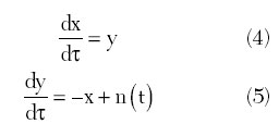
From Equations 4 and 5, it follows that the instantaneous change of the ordinate y by a value of dny = nd? will occur, due to the small external force injected into the oscillation system. This corresponds to a step change of the representative point M0 from the position K to the position L, resulting in the amplitude and phase changes, as shown. These changes can be determined from the consideration of a triangle KLN by
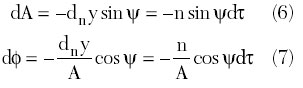
Thus, the separate first-order differential equations for the time-varying amplitude and phase can be obtained from Equations 6 and 7 as

Since the right-hand sides of Equations 8 and 9 are small, time-averaged differential equations can be used instead of the differential equations for the instantaneous values of the amplitude and phase. Hence, the changes of the amplitude and phase for a time period t ? T are defined as

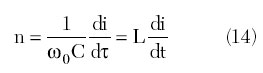
Figure 2 shows the equivalent circuit of the negative resistance oscillator with an injected small perturbation current i(t). In a steady-state oscillation mode, when the losses in the resonant circuit are compensated by the energy inserted into the circuit by the active device, the second-order differential equation of the oscillator is written as

where ?0 = 1?LC is the resonant frequency and v(t) is the voltage across the resonant circuit. If a current impulse i(t) is injected, the amplitude and phase of the oscillator will have time-dependent responses. According to Equations 10 and 11, the resultant amplitude and phase changes have a quadrature dependence with respect to each other. When an impulse is applied at the peak of the voltage across the capacitor, there will be a maximum amplitude deviation with no phase shift (b). On the other hand, if the current impulse is applied at the zero crossing, it will result in a maximum phase deviation with no amplitude response, as shown in (c).

Fig. 2 Second-order LC oscillator and the effect of an injected impulse.
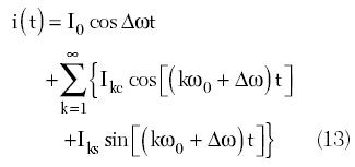
Suppose that a perturbation current i(t), injected into the oscillation circuit, is a periodical function that can generally be expanded into a Fourier series
where
I0 = DC component of the current
Ikc = kth cosine current harmonic amplitude
Iks = kth sinusoidal current harmonic amplitude and ?? << ?0
In this case, the small external force can be redefined as
Consequently, substituting Equation 13 into Equations 10 and 11 and taking into account that ?0 + ?? ? ?0 results in
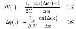
where V is the voltage amplitude across the capacitor C. In this case, only the fundamental components of the injected current i(t) can contribute to the amplitude (sine amplitude) and phase (cosine amplitude) fluctuations given by Equations 15 and 16, because for the DC and kth-order current components, the arguments for all their integrals in Equations 10 and 11 are significantly attenuated by the averaging over the integration period.
The output voltage of an ideal cosine oscillator with constant amplitude V and phase fluctuations ?? can be written as

resulting in an output spectrum of the oscillator with sidebands close to the oscillation frequency ?0. Since, for a narrowband phase modulation with small phase fluctuations, sin [??(t)] ?@ ??(t) and cos [??(t)] ? 1, the phase modulation spectrum given by Equation 17 can be rewritten by using Equation 16 as

which is similar to the single-tone amplitude modulation spectrum containing the spectral components corresponding to the carrier frequency ?0 and two close sideband frequencies ?0 – ?? and ?0 + ??.
The injection of the current

has similar effect, resulting in twice the noise power at the sidebands. Therefore, an injected total current i(t) results in a pair of equal sidebands at ?0 ± ?? with a sideband power Psb relative to the carrier power Pc given by
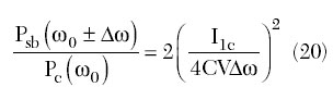
Now let us assume that a stationary thermal noise current with a white power spectral density i2n is injected into the oscillator circuit close to carrier. Then, by making a replacement between the amplitude and root-mean-square current values when i21c/2 = i2n, the single sideband power spectral density for the phase fluctuations at ?? offset from the carrier ?0 in the 1/f region can be written using Equation 20 as

Taking into account that i2n= 4FkT/RL for ?f = 1 Hz, QL = ?0CRL and PL = V2/2RL, where RL is the tank parallel or load resistance, Equation 21 can be rewritten as
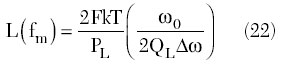
which is similar to the one for the negative resistance oscillator (see Equation 26 in Part II2).
Effect of Higher Order Harmonics
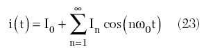
Generally, the transition from soft start-up oscillation conditions to steady-state self-sustained oscillations is provided as a result of the degradation of the device transconductance in a large-signal mode, when the active device operates in both pinch-off and active regions. As a result, for the cosine voltage across the resonant circuit, the output collector (or drain) current i(t) represents a Fourier series expansion
where
I0 = DC current
In = amplitude of the nth harmonic component
If the oscillation frequency is equal to the resonant circuit frequency, which means that the active device has no effect on the oscillation frequency, then the fundamental component of the collector voltage will be in phase with the fundamental component of the collector current. However, for all higher order voltage harmonics the impedance of the resonant circuit will be capacitive since the collector current harmonics are mostly flowing through the shunt capacitance. Therefore, for the Meissner oscillator circuit shown in Figure 3, the voltage at the input of the active device can be approximately represented as
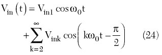
where Vink << Vin1 for a high value of the oscillator loaded quality factor.

Fig. 3 Schematic of a parallel feedback oscillator.
In this case, when the active device’s transfer characteristic is approximated by a second-order polynomial i(t) = a0 + a1vin + a2v2in and the input voltage vin(t) in Equation 24 is limited to the first two factors when k = 2, the output fundamental current corresponding to the two-harmonic input voltage can be written as

where I1 = gmVin1, gm = a1 is the average transconductance for cosine input voltage. Equation 25 can be rewritten in the form of
![]()
From Equation 26, it follows that the presence of the second-order voltage harmonic contributes, first to the changes in the fundamental amplitude (I1 ? I'1) and average transconductance
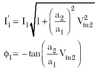
and second, to the appearance of the phase shift ?1 between the fundamental current and fundamental voltage. The latter means that the device transconductance becomes complex due to the effect of the higher order harmonics and its magnitude and phase depend on the harmonic level. For example, an increase of the harmonic level results in a decrease in the oscillation frequency.
Physically, the influence of the harmonic content on the frequency variation can be explained as follows: if the oscillations are purely sinusoidal, the energy distribution in both arms of the resonant LC-circuit is equal; when the harmonics appear, the currents corresponding to them flow mainly through the capacitive arm, and therefore they increase the electrostatic energy of this arm in comparison with the inductive arm; in order to keep the energy equal in both arms, the fundamental frequency must slightly decrease with respect to the frequency given by the tank circuit only.7
In a general form, the frequency deviation ??, caused by the presence of harmonics of the voltage v on the resonant circuit, can be obtained from
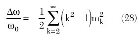
where k is the order of harmonic and mk = Vk/V1 is the ratio of the harmonic voltage component to the fundamental voltage.7
In view of the multiharmonic representation of the oscillator output spectrum due to the device and resonant circuit nonlinearities, the total phase fluctuations can be represented by a superposition integral as a result of each harmonic contribution. This is similar to the Fourier harmonic expansion in the frequency domain of the voltage waveform, when the phase trajectory on the phase plane is a result of the phase trajectories with different radii and velocities corresponding to the DC shift and harmonic amplitudes. In this case, Equation 11 can take the general form

where

in a dimensionless periodic function characterizing the shape of the limit cycle or phase trajectory corresponding to the oscillation waveform and depending on the oscillator topology. It is called the impulse sensitivity function (ISF) for an approximate model for the oscillator phase behavior3 and serves a similar role at the perturbation projection vector (PPV) for the exact model.8 The initial phase ?n in Equation 30 is not important for random noise sources and can be neglected. For an ideal case of a purely sinusoidal oscillator, c1 = 1 and ?(t) = cos?0t. Now if any stationary noise current with a white power spectral density i2n/?f is injected into the oscillator circuit close to any harmonic n?0 + ?? or n?0 – ??, it will result in a pair of equal sidebands at w0 ± ?w. Then, the total single sideband power spectral density for the phase fluctuations in a bandwidth ?f= 1 Hz can be written, based on Equation 21, as

where ?rms is the root-mean-square value of ?(t).4 Thus, the total noise power near the carrier frequency of the oscillator is a result of the up-converted 1/f noise near DC, weighted by coefficient c0, the noise near the carrier weighted by coefficient c1 and the down-converted white noise near the second- and higher order harmonics weighted by coefficients cn, n = 2,3,…. The converted phase noise due to the conversion from one sideband to another can be of the order of 6 dB higher than the additive noise in the oscillator.9
From Equation 31, it follows that the effect of the converted phase noise can be reduced by minimizing the DC coefficient c0 and the higher order harmonic coefficients cn, n =2, 3,…, of the (?), approximating the cosine waveform of the injected node voltage. Figure 4 shows the voltage waveforms corresponding to (a) class F with flattened waveform consisting of the fundamental and third harmonics only and (b) inverse class F consisting of the fundamental and second harmonics only.10 To realize the symmetrical flattened voltage waveform, the ratio between the fundamental and third harmonic should be equal to V1/V3 = 9, while the ratio between the fundamental and second harmonic is equal to V1/V2 = 4 for the symmetrical waveform close to the half-cosine shown. Hence, the level of higher order harmonics is significantly smaller for the symmetrical flattened voltage waveforms. It should be noted that, in class E operation with a non-symmetrical voltage waveform, the effect of the second- and higher order harmonics is significant, resulting in a high value of the voltage peak factor. The importance of the symmetry is necessary also to minimize the coefficient c0 responsible for the low noise up-conversion and amplitude-to-phase conversion.3 A phase noise improvement can be achieved by reducing the effect of the device and circuit nonlinear capacitances (see Part II,2 Equation 42). Due to the amplitude-to-phase conversion, the phase for each higher order harmonic changes with amplitude resulting in a generally asymmetrical voltage waveform.

Fig. 4 Voltage waveform for n harmonic peaking.
Equation 29 describes an approximate phase noise behavior, compared with the accurate equation given by Demir, et al.,8 where the phase of ?(t) also appears in its right-hand side. Such a simplified phase noise model is valid for the case of stationary noise sources like white noise. However, when the noise sources are no longer stationary, it can be accurate only in the limits of an assumption of the small phase shifts for which cos ?? is close to unity. This implies that the approximate model is not accurate enough to analyze neither injection-locking phenomenon nor related issues like the behavior of phase differences of coupled oscillators.11
The response of the oscillation system to an impulsive noise can be provided by its direct measurement with a SPICE simulator, when an impulse is injected into the node of interest of the oscillator circuit and the oscillator simulated for a few cycles afterwards.3 By substituting the equivalent current noise source of each individual node in Equation 29, the phase contribution of each node can be calculated.12 However, any further analytical simplification based on the orthogonal decomposition of noise into amplitude and phase components may not yield the correct result.13
Cyclostationary Noise
The noise sources in an oscillator generally cannot be modeled only as stationary since the statistical properties of some of them may change with time in a periodic manner. Such types of noise sources are referred to as cyclostationary. If the thermal noise of the resistor has a stationary nature, then the collector (or drain) shot noise of the transistor is an example of cyclostationary noise due to the time-varying nature of the collector current. The most important issue is that the collector shot noise is dominant, compared to the noise from the base resistance or tank losses, and can contribute approximately 70 percent of the total phase noise of the oscillator.12
Figure 5 shows a simplified, single-ended, common gate CMOS Colpitts oscillator configuration where the required regeneration factor for the start-up oscillation conditions is chosen using a proper ratio of the feedback capacitances C1 and C2. The idealized voltage and current waveforms corresponding to the large-signal operation in idealized class B with zero saturation voltage are shown in Figure 6.

Fig. 5 Simplified Colpitts oscillator schematic.

Fig. 6 Ideal class B drain voltage and current waveforms.
Equation 23, or the drain time-varying current, can be rewritten in the form of

where ?n is the ratio of the nth harmonic current amplitude to the peak output current Imax, expressed through half the conduction angle ? as

where
?n(?) = current coefficients
To account for the cyclostationary drain noise source as a result of total noise sources injected at frequencies n?0 ± ??, Equation 31, in a general form, can be rewritten as

where i2nd = 2qImax is the drain current noise power density in a frequency bandwidth ?f = 1 Hz. The Fourier components for the current waveform close to half-cosinusoidal show that the drain shot noise is mixed mostly with the fundamental and second harmonics to contribute to the total phase noise of the oscillator.
To minimize the oscillator phase noise, it is very important to choose the optimum value of the feedback ratio k = C2/C1 for the same total capacitance C = C1C2/(C1 + C2). This is because different values of the conduction angle correspond to different harmonic contribution to the output spectrum. In the case of class B with ? = 90°, the third-, fifth- and higher order harmonics can be eliminated since their current coefficients ?n (for n = 3,5,…) become equal to zero. As a rule-of-thumb, the optimum feedback ratio for a Colpitts oscillator can be chosen to be approximately k = 3.5 to 4.3,12
Conclusion
The impulse response model for the oscillator phase noise, which has become popular recently, is explained based on a well-known phase plane approach. This model specifies the contribution of the noise components located near integer multiples of the oscillation frequency in terms of waveform properties and circuit parameters. By using this nonlinear approach, it is impossible to derive an explicit relationship between the oscillator stability conditions, amplitude-to-phase conversion and phase noise power density, unlike with the Kurokawa approach. Such an approach, however, based on the inherent time-varying nature of the oscillator, provides an important design insight by identifying and quantifying the major sources of phase noise degradation.
References
1. A. Grebennikov, “Transistor LC Oscillators for Wireless Applications: Theory and Design Aspects, Part I,” Microwave Journal, Vol. 48, No. 10, October 2005, pp. 62–78.
2. A. Grebennikov, “Transistor LC Oscillators for Wireless Applications: Theory and Design Aspects, Part II,” Microwave Journal, Vol. 48, No. 11, November 2005, pp. 62–82.
3. A. Hajimiri and T.H. Lee, “A General Theory of Phase Noise in Electrical Oscillators,” IEEE Journal of Solid-State Circuits, Vol. 33, February 1998, pp. 179–194.
4. T.H. Lee and A. Hajimiri, “Oscillator Phase Noise: A Tutorial,” IEEE Journal of Solid-State Circuits, Vol. 35, March 2000, pp. 326–336.
5. A.A. Andronov, A.A. Vitt and S.E. Khaikin, Theory of Oscillations, Dover Publications, New York, NY, 1987.
6. K.A. Samoylo, Method of Analysis of Second-order Oscillation Systems, Moskva: Sov. Radio, 1976.
7. J. Groszkowski, “The Interdependence of Frequency Variation and Harmonic Content, and the Problem of Constant-frequency Oscillators,” Proceeding of the IRE, Vol. 21, July 1933, pp. 958–9813.
8. A. Demir, A. Mehrotra and J. Roychowdhury, “Phase Noise in Oscillators: A Unifying Theory and Numerical Methods for Characterization,” IEEE Transactions on Circuits and Systems I: Fundamental Theory and Applications, Vol. I-47, April 2000, pp. 655–673.
9. J.C. Nallatamby, M. Prigent and J. Obregon, “On the Role of the Additive and Converted Noise in the Generation of Phase Noise in Nonlinear Oscillators,” IEEE Transactions on Microwave Theory and Techniques, Vol. 53, No. 3, March 2005, pp. 901–906.
10. A. Grebennikov, RF and Microwave Power Amplifier Design, McGraw-Hill, New York, NY, 2004.
11. P. Vanassche, G. Gielen and W. Sansen, “On the Difference between Two Widely Publicized Methods for Analyzing Oscillator Phase Behavior,” Proceedings of the IEEE/ACM International Conference on Computer Aided Design, 2002, pp. 229–233.
12. M.A. Margarit, J.L. Tham, R.G. Meyer and M.J. Deen, “A Low Noise, Low Power VCO with Automatic Amplitude Control for Wireless Applications,” IEEE Journal of Solid-State Circuits, Vol. 34, June 1999, pp. 761–771.
13. G.J. Coram, “A Simple 2-D Oscillator to Determine the Correct Decomposition of Perturbations into Amplitude and Phase Noise,” IEEE Transactions on Circuits and Systems I: Fundamental Theory and Applications, Vol. I-48, July 2001, pp. 896–898.