
 There has always been a critical need to measure and control RF power in wireless communication networks. Accurate measurement and control aids in the setting of overall cell coverage, and ensures that the RF power amplifiers in the wireless base station are operated for optimum thermal performance. In early cellular networks such as GSM (1G/2G) and AMPS cellular systems, for example, transmitter RF power could be easily measured using a pair of Schottky diodes: one for peak power detection, and the other for temperature compensation. This technique was adequate since the ratio of the peak power to the average power being measured did not vary significantly. Later, various types of logarithmic detectors were used and these were also found to provide acceptable performance in most situations.
In recent years, the applications for wireless broadband services have continued to expand at a high rate. To keep pace with this demand, wireless communications networks must continue to provide higher data transmission rate capability. In order to do this in an efficient manner, wireless communications technology has relied upon ever more complex bandwidth efficient modulation schemes.
The evolution of complex digital modulation schemes such as QPSK, 8PSK, 16QAM and OFDM means that a greater amount of data or bits/second can be transmitted in a given bandwidth, with the disadvantage being that much more complex circuitry in the form of DSP hardware and software algorithms, wide dynamic range modulators and demodulators, and higher linearity RF power amplifiers is required to handle these signals. Another disadvantage of these complex digital modulation waveforms is that RF power measurement and control becomes more difficult.

The reason for this is that contemporary wireless base stations are transmitting RF signals whose peak-to-average value (also defined as crest factor) is constantly changing. This varies widely depending on the number of calls being processed by the base station, and also with the differing power levels transmitted by multiple service providers. For example, base stations in 3G CDMA-based systems transmit downlink signals with crest factors as high as 15 dB for single carrier systems, and 20 dB for base stations with multiple CDMA carriers. Figure 1 shows an example of an implementation of a wireless base station transmitter solution.
It should also be noted that there is a requirement in many types of digital receivers to measure and control the gain of the received signal. This is commonly referred to as the RSSI (Received Signal Strength Indicator). This serves to prevent overdriving the IF amplifier stages and analog-to-digital converters further downstream on the receive channel.

In order to meet the need for power measurement in the challenging environment of high data rate wireless infrastructure applications, Hittite Microwave has released the HMC610LP4E SiGe BiCMOS true RMS power detector. The HMC610LP4E sets a new performance benchmark by providing wide dynamic range RMS signal power measurement in excess of 70 dB. The new detector product converts any RF input signal at its differential input, regardless of modulation or waveform complexity, to an accurately scaled linear-in-dB output response that represents the RMS value of the input waveform (see Figure 2.)
The HMC610LP4E delivers extremely high dynamic range over an input RF frequency range of 50 Hz to 3.9 GHz, covering all of the cellular/3G, WiMAX and WiBro bands. The HMC610LP4E delivers a ±1 dB linear in dB dynamic range of 70 dB at 900 MHz. At 2.7 and 3.5 GHz, the new detector extends the current benchmark by providing ±1 dB dynamic ranges of 63 and 56 dB, respectively. At 3.9 GHz, the ±1 dB dynamic range is still very useable at 42 dB.
The HMC610LP4E has been successfully tested with many different input waveforms over a wide range of input frequencies (see Figure 3). It accurately converts a wide range of RF input waveforms with different modulations at 3 GHz over a –50 to +5 dBm input power level range. Figure 4 clearly shows that with single and multiple carrier versions of WCDMA, CDMA2000 and IS95 reverse link, the HMC610LP4E typically exhibits less than 0.3 dB of error versus modulation waveform up to input power levels of +5 dBm.
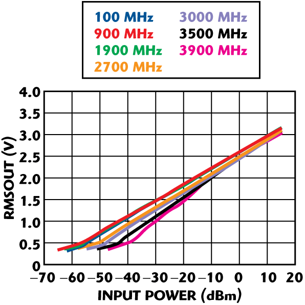
For normal operation, the RMSOUT pin is shorted to the VSET input, and will provide a nominal logarithmic slope of 37 mV/dB and an intercept of –70 dBm for frequencies up to 2 GHz. Both the nominal logarithmic slope and the intercept are temperature and supply stable. Other logarithmic slopes are achieved with external resistors connected between RMSOUT and VSET pins. Typical output voltage range is from +0.4 to +3.2 V. Temperature stability is excellent with ±0.5 dB error from –40° to +85°C, which is maintained for input frequencies from 100 MHz to 3.9 GHz.
The minimum output rise time (0.2 to 1.9 V) of the HMC610LP4E is 10 ns, and the fall time (1.9 to 0.2 V) is 500 ns, which is ideal to support the proper detection of wireless broadband modulation schemes. The RF input of the HMC610LP4E is externally matched to 50 Ω, and the device operates from a single +5 V supply consuming between 65 and 85 mA, depending on input power level which can vary from –70 to +15 dBm. The ENX pin is connected to ground for normal operation, but when a DC signal of +5 V is applied, the device will power down to 5 mW. The HMC610LP4E powers up within 2 μs to its nominal operating current of 65 mA at 25°C.
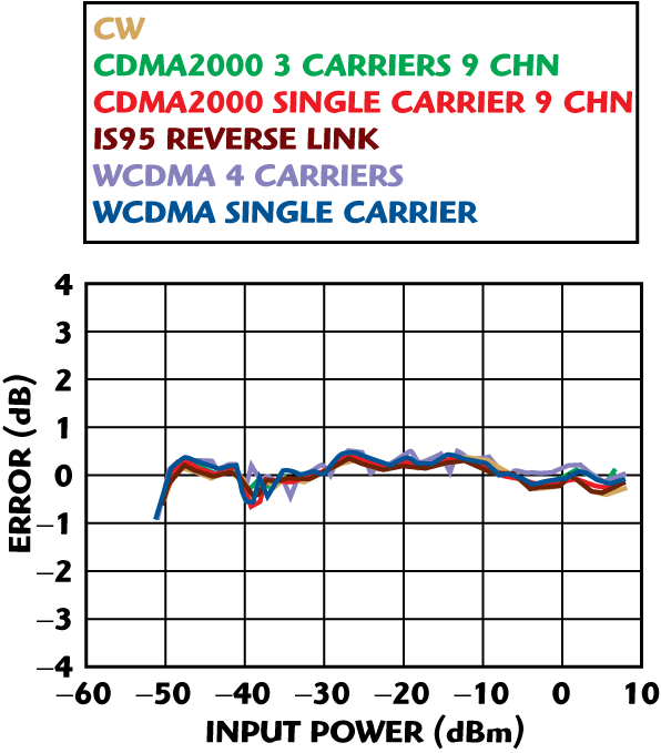
Figure 5 shows an example of how the HMC610LP4E may be combined with other Hittite components to construct a circuit suitable for measuring RMS power in the transmit channel of a wireless base station. The simplified block diagram shows how the HMC610LP4E power detector can be used to construct an AGC loop in a transmit RF chain. In this example, the HMC552LP4E, which is a 1.6 to 3.0 GHz double-balanced mixer, is used to upconvert the transmit IF signal. The RF output of the HMC552LP4E is routed through the HMC473MS8 voltage variable attenuator and then coupled into the RF input of the HMC610LP4E. The DC output of the HMC610LP4E, which represents the RMS power in the transmit signal path, is compared with the Vreference value at the other input of the op-amp, and provides feedback control to the HMC473MS8 voltage variable attenuator. The HMC473MS8 accepts a single positive control voltage, and provides an attenuation range of up to 48 dB. This loop ensures that the appropriate signal level is applied to the HMC482ST89 gain block amplifier, and to the subsequent RF amplification stages.
Conclusion
A new RMS power detector operating from 50 Hz to 3.9 GHz extends the performance of currently available devices, providing a linear-in-dB transfer function with linearity of ±0.6 dB typical, over an input power range of more than 60 dB. In short, the HMC610LP4E provides wireless infrastructure designers with the means to reduce the design complexity of high data rate systems requiring the measurement of RF signals with high crest factors.

Hittite Microwave also provides a wide range of compatible products to meet the needs of wired and wireless infrastructure applications. These products, together with the HMC610LP4E RMS power detector, its evaluation PC board and each of the products shown in the block diagrams (Figures 1 and 5) are available from stock and can be ordered via the company’s e-commerce site, or via direct purchase order. Released data sheets and S-parameter data are available on-line at www.hittite.com.
Hittite Microwave Corp.
Chelmsford, MA
(978) 250-3343
www.hittite.com
RS No. 302