
Baseband digital predistortion based on the LUT is a popular method to improve the performance of high power amplifiers. The feedback loop is the key unit to obtain the sampled signals based on which the model of the PA is built.
The imperfectness of the modulator and demodulator will influence the signal performance. The nonideal characters of the demodulator will limit the improvement of the predistortion. In this paper, error items of the demodulator in the feedback path are analyzed and the compensating algorithm is derived.[1] Also the simulation is completed to validate the closed-form algorithm in the numerical way.
Background and Retrospect
Advanced current and future mobile communication systems are required to achieve very high data rate to make the broadband applications realizable. Therefore, complicated digital modulation techniques such as 16QAM, 64QAM, etc., are adopted in such systems to enhance the spectrum efficiency. Accordingly, power amplifiers built in the basestations of those systems need to be characterized by high linearity and efficiency to meet the large peak-to-average ratio of the high order digital modulated signals. Linearization techniques such as the feed-forward method, RF predistortion method , digital predistortion method, etc., are usually used to enhance the linearity and the efficiency of the power amplifiers.
For the feed-forward linearization method [2], it is quite difficult to precisely control the amplitude and phase of the compensating RF signals added to the origin distorted signals. For the RF predistortion linearization method, the inverse functions of the power amplifiers are difficult to realize exactly, which will limit the linearity improvement. Baseband Digital predistortion linearization methods based on LUT table [3] modify the baseband signals directly to ameliorate the linearity of the amplified RF signals. In order to explain the error analysis more clearly, a simplified block diagram of a typical digital predistortion system [4] is shown in Fig. 1.

Fig. 1. Simplified diagram of baseband digital predistortion
The procedure of the DPD is described in [3]. During the training stage, digital I and Q data of training signals are converted to the analog I and Q signals by the DACs. After that I and Q signals are modulated to the RF band by a direct quadrature modulator. The modulated signal is sent to the driver amplifier and the power amplifier under the test and linearization. The amplified and distorted signal is coupled into the downconvertor and then is demodulated to base band I’ and Q’ signals. ADCs are used to digitalize the I’ and Q’ signals. By comparing the original I and Q data and the digitalized I’ and Q’ data, the nonlinearity of the power amplifier can be estimated, based on which the digital predistortion can be realized. The mechanism of the predistortion is to change the characteristics of the baseband signals to compensate the distortion caused by the power amplifier in advance. It’s obvious that the modulator and the demodulator are very important devices in the predistortion loop. Imperfect modulators and demodulators will cause some additional distortions to such system. Some of those distortions aroused in the feedback route should not be regarded as the congenital characteristics of the power amplifier.
In this paper, the effect of the modulation and demodulation errors on the modeling of the power amplifiers is analyzed. To overcome the effect of those errors, a straightforward algorithm is derived for ideal demodulation.
Analysis and Derivation
The feedback loop is an important unit in the Baseband Digital Predistortion system based on the LUT method. Demodulators are the key components in the feedback loop. It converts the coupled output signals to the analog baseband I and Q signals. Since signals transmitted from the base stations are normally band limited and with few spurious emissions, direct demodulators are adopted here to simplify the feedback loop structure. According to the sampled feedback signal with the non-linear distortion using AD convertors and the directly sampled baseband signals without non-linear distortion, the LUT data used to modify the digital baseband signals are obtained. The quadrature modulation process of the transmitting path and demodulation process of the feedback loop in the Fig. 1 can be simplified as Fig. 2. Here, EMBED Equation.3 is the signal phase shift on the RF channel between the transmitting and receiving ports. It is a determinate value caused by the passive coupler, microstrip lines, amplifiers, etc., which can be estimated and compensated at the receiving end.
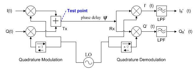
Fig. 2. Analog quadrature modulation and demodulation
If the modulator is an ideal one which means that the amplitude error and phase error are zeros. The modulated signal from the ideal modulator can be expressed as,
R(t) = A1I(t)cos(ωct + φ1) - A1Q(t)sin(ωct + φ1) (1)
Where A1 is the amplitude gain of the quadrature modulator and φ1 is the phase shift caused by the modulator. For the purpose of simplicity, the coupling coefficient of the coupler is assumed to 1. Thus, according to the Fig.2, after the radio frequency channel including the coupler, the modulated signal fed to the demodulator is
R'(t) = A1I(t)cos(ωct + φ1 + ψ) - A1Q(t)sin(ωct + φ1 + ψ) (2)
If the demodulator is also an ideal one, the output of the ideal demodulator is
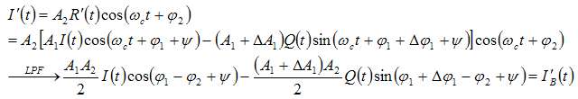
 (3)
(3)
 (4)
(4)
Where A2 is the amplitude gain of the quadrature demodulator and φ2 is the phase shift caused by the demodulator.
However, actually, general quadrature modulators and demodulators available are not ideal devices [5]. Amplitude errors and phase errors of modulators and demodulators will introduce additional distortion to the modulated and demodulated signals. The amplitude error of the modulator or the demodulator is the amplitude difference between the in-phase and quadrature paths of the modulator or the demodulator. Similarly, the phase error of the modulator or the demodulator is the difference of the phase shift between the in-phase and quadrature paths of the modulator or the demodulator. Assume that the amplitude error of the modulator is ΔA1 and the amplitude error of the demodulator is ΔA2. The phase error of the modulator is Δφ1 and the phase error of the demodulator is Δφ2.
Therefore, in the case of using nonideal modulators and demodulators, (2), (3) and (4) should be rewritten as (5), (6) and (7)
 (5)
(5)
 (6)
(6)
 (7)
(7)
Errors in received I'B(t) and Q'B(t) signals are
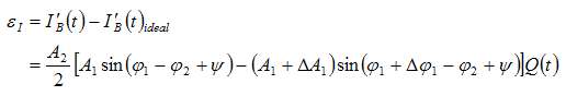 (8)
(8)
 (9)
(9)
Apparently, error items ΕI and ΕQ in (8) and (9) include the nonideal characters of the modulator and demodulator, which will cause the unbalance of the received I'B(t) and Q'B(t). Since building the PA model is essentially based on the I'B(t) and Q'B(t) from the feedback loop of the system, the ΕI and ΕQ will affect the accuracy of the model in some degree and will eventually limit the improvement of the linearity of the PA. According to the Fig. 1 , the transmitting path includes the modulator, driver and PA while the path of training series includes the modulator, driver, PA, demodulator and the low-band pass filters. That is to say, the training signals not only carry the error information from the transmitting path which the normal signals undergo, but also carry the error information from the feedback path which has no relationship with the transmitting path. Therefore, the imperfectness of the demodulator in the ΕI and ΕQ can not be compensated by the DPD processing unit and it is the certain error to be eliminated by this algorithm.
In order to eliminate the error items of the nonideal demodulator, a test signal can be input into the feedback path to calculate the ΔA2 and Δφ2 which stand for the unbalance characters of the in-phase and quadrature paths of the demodulator. Suppose that an RF continuous wave signal stest(t) = cos(ωct - ωst) is fed to the feedback path at the test point which is indicated in Fig. 2. Assume that during the test and self-correction stage, no other normal signals are fed into the transmitting path. Such interfering free conditions for test and self-correction can be realized by mechanical switching and software controlling. The received test RF and demodulated signals in feedback path described in equations (5), (6) and (7) are
 (8)
(8)
 (9)
(9)
 (10)
(10)
During the test and self-correction stage, the value arrays of I'B test(t) and Q'B test(t) can be obtained from AD converters in the feedback path. Therefore, using the Fourier transformation, A'I B test(t), A'Q B test(t), α'I B test, α'Q B testcan be obtained and regarded as knowns. With that, ΔA2 and Δφ2 can be calculated with
 (11)
(11)
With the calculated error parameters ΔA2 and Δφ2, a compensating unit can be inserted into the feedback path between the AD converters and predistortion processing unit as shown in Fig. 3. Where,  and
and  denote compensated signals.

Fig. 3 Diagram of the modified baseband digital predistortion system.
According to equations (6) and (7), the relations among  and
and  can be deduced and expressed in (12).
 (12)
(12)
Therefore, with the relations (12), compensated or corrected baseband signals data arrays I"B(t) and Q"B(t) can be obtained from I'B(t) and Q'B(t) data arrays.
 (13)
(13)
Where, according to the above description, ΔA2 and Δφ2 are knowns. It is obvious that after the compensation or correction, the imperfectness of the demodulator will be eliminated. Thereby, a more accurate model of PA can be built based on the corrected data.
Simulation
According to the analysis and deduction above, the closed-form relations, expressions and corrections of the error items are provided. For the purpose of practical realization, simulations of the parameters extraction and signal data correction in numerical data form have been completed by the tool Matlab.
In the simulation, 16QAM modulated signal is generated and modulated to the RF carrier at 1024MHz. The symbol rate is 128Msps. Fig. 4(a) shows the 16QAM baseband signal constellation. Fig. 4(b) is the 16QAM baseband signal with shaped raised cosine FIRs. Fig. 4(c) is the 16QAM modulated RF signal in time domain while Fig. 4(d) is the modulated RF signal spectrum. In order to make the problem clearer in the simulation, we assume that ΔA1 = 0 and Δφ1 = 0 which mean that the modulator is an ideal one and also we assume that the RF phase shift Ψ = 0.
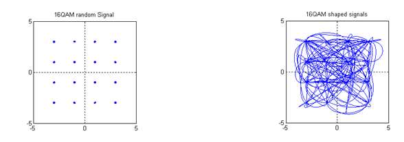
Fig. 4(a) 16QAM baseband signal. Fig. 4(b) 16QAM signal with shaped raised cosine FIRs

Fig. 4(c) 16QAM modulated RF signal Fig. 4(d) 16QAM modulated RF signal spectrum Fig. 4 16QAM modulated signals
A nonideal demodulator is used in the simulation. Although normally the amplitude error has a centesimal scale and the phase error is a few degrees for analog demodulator, we presume that ΔA2 = 0.2 and ΔΦ2 = 15° to have a clearer view of the effect. During the test and correction stage, a test continuous wave (CW) signal at the frequency 1016MHz (8MHz offset from the RF carrier) is added to the test point in the simulation.
Fig. 5(a) shows the received test RF CW signal at the frequency of 1016MHz. Fig. 5(b) is the directly demodulated test baseband signal constellation. Since the test signal is a CW, the demodulated signal should be a circle on the constellation. The mussy lines are caused by the mirror mixed signal at 2040MHz. Fig. 5(c) is the modulated test baseband signal constellation filtered with a low-pass filter to get rid of the mirror spurious frequency. With the nonideal characters of the demodulator, the circle appears as an askew ellipse.
In fact, parameters ΔA2 and ΔΦ2 are unknown for the processing unit when given demodulated data arrays. In the simulation, demodulated test signal frequency is distinguished from the FFT data. The amplitude and phase of the indexed demodulated in-phase and quadrature signals are obtained. Then, ΔA2 and ΔΦ2 can be calculated using equation (11). Here, the calculated results are ΔA2 = 0.2000 and ΔΦ2 = 15.0015° which are almost identical with the previous parameters when generating the demodulated data. With the known nonideal parameters of demodulator, the corrected data array can be obtained using equation (13). The result is shown in Fig. 5(d). The nonideal characters are compensated and corrected. A pretty normal circle is obtained.

Fig. 5(a) Received test RF CW signal Fig. 5(b) Demodulated test signal without LPFs

Fig. 5(c) Demodulated test signal with LPFs Fig. 5(d) Corrected demodulated signal Fig. 5 Modulation, demodulation, parameters extraction and correction of the test signal
Similarly, Fig. 6(a) shows the directly demodulated 16QAM signal constellation. The mussy lines are caused by the mirror mixed signal centered at 2048MHz. Fig. 6(b) is the directly demodulated 16QAM signal spectrum with the mirror mixed signal existing. Fig. 6(c) is the modulated 16QAM signal filtered with a low-pass filter. With the nonideal parameters obtained in the above-mentioned test signal stage, the 16QAM demodulated signal can be compensated and corrected using equations (13). The corrected demodulated signal is shown in Fig. 6(d) which is identical with the modulated signal in Fig. 4(b).
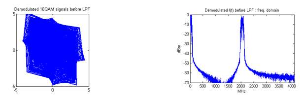
Fig. 6(a) Demodulated 16QAM signal without LPFs Fig. 6(b) Demodulated 16QAM signal spectrum

Fig. 6(c) Demodulated 16QAM signal with LPFs Fig. 6(d) Corrected 16QAM demodulated signal Fig. 6 Demodulation and correction of the 16QAM signal
The simulation details the total data processing procedure for demodulation, parameters extraction and signal data correction. Perfect consistence is achieved between the deduction and the numerical calculation.
Conclusions
In this paper, quadrature modulated and demodulated signal components are analyzed. It is indicated that the performance of the modulator and demodulator will influence the amplitude and the phase balance of the signal. Due to the position of the demodulator, its nonideal characters will affect the effect of the baseband digital predistortion obviously. Here, unbalanced items in amplitude and phase of the demodulator ΔA2 and ΔΦ2 are calculated and relations among I"B(t), Q"B(t) and I'B(t), Q'B(t) are derived. Simulations are carried out to realize the closed-form derivation with numerical calculations and the results are quite good.
According to the analysis, derivation and simulation presented above, error items caused by the imperfect demodulator in the feedback path can be eliminated and the corrected demodulated data can be obtained. In practice, training signals are sent from the DPD processing unit. The information carried by the distorted training signals contains the nonlinear characters introduced by the power amplifier and the nonideal characters of the transmitting path including the modulator but the demodulator. The additional compensating unit based on the algorithm above eliminates error items in the feedback data arrays which are mainly introduced by the demodulator. That will provide the DPD processing unit cleaner data arrays of the feedback training signals. As a result, the more precise nonlinear model of the power amplifier can be obtained using curve fitting at the DPD processing unit. After that, the DPD processing unit transforms the incoming baseband data using inverse function of the model to optimize the linearity. Based on the improved DPD method, the practical hardware platform can be realized.
REFERENCES
1. Jianing Zhao, Jianyi Zhou, Ningde Xie, Jianfeng Zhai, and Lei Zhang, “Error Analysis and Compensation Algorithm for Digital Predistortion Systems,” Progress In Electromagnetics Research symposium (PIERS) 2007, Beijing, China, vol.2, no. 6, pp.702-705, 26th-30th March 2007
2. Jianyi Zhou, Lei Zhang, Wei Hong, Jianing Zhao and Xiaowei Zhu, “Design of a Wideband Adaptive Linear Amplifier with a DSB Pilot and Complex Coherent Detection Method”, Microwave Journal, vol. 49, no. 4, pp. 104-114, April 2006
3. Jianyi Zhou, Shi Ming, Jianing Zhao, Chen Ming, and Lei Zhang, “An Adaptive Baseband Digital Predistortion System for RF Power Amplifier: Design, Hardware and Software Realization, and Experimental Test”, Microwave Journal, to be published
4. Ming Shi; Ming Chen; Lei Zhang; Jianyi Zhou, “A new baseband digital predistortion system,” Microwave Conference Proceedings (APMC) 2005, SuZhou, China, vol. 2, 4th-7th Dec. 2005
5. Li, M.Y.; Deng, J.X.; Larson, L.E.; Asbeck, P.M. “Nonideal effects of reconstruction filter and I/Q imbalance in digital predistortion,” Radio and Wireless Symposium, 2006 IEEE, pp. 259 – 262, 17th-19th Jan. 2006