

Among the various kinds of wireless communication systems, wireless LAN (WLAN) is the most popular for short-range communications, due to its high data rate. For low cost and low power implementation of a WLAN terminal, a fully integrated CMOS RF transceiver is required for which a low- or zero-IF (direct-conversion) architecture is best suited because the number of external components is minimized1-2.
A low-IF architecture provides a much higher immunity for DC-offset and flicker noise than a direct-conversion architecture, but a high-level of matching between signal paths is required for sufficient image rejection3. The 5 GHz WLAN standard, IEEE 802.11a, uses OFDM, where the first sub-carrier is not used and the channel bandwidth is wide4. Therefore, it is relatively immune to DC-offset and flicker noise and a direct-conversion receiver architecture has been a popular choice1-2.
In this article, a fully integrated CMOS direct-conversion receiver, including a frequency synthesizer, is described for 5 GHz WLAN applications. Sub-harmonic mixing minimizes the DC-offset and the residual DC-offset of the baseband circuits is compensated by a digital-to-analog converter (DAC).
The octa-phase local oscillator (LO) signals, required for quadrature sub-harmonic mixing, are generated by an integer-N type frequency synthesizer. The architecture and circuit implementation of the receiver are described and the detailed experimental results are given.
Direct-conversion Receiver with Sub-harmonic Mixing
The overall block diagram of the 5 GHz direct-conversion receiver is shown in Figure 1. The bandgap reference (BGR) generates the required bias voltages and currents for each block. The serial port interface (SPI) is used to provide the various control signals such as gain-control of the low-noise amplifier (LNA) and programmable gain amplifier (PGA).
To minimize the DC-offset due to LO self-mixing, sub-harmonic mixing is used for down-conversion. The residual DC-offset of the baseband circuits is cancelled by a DAC at the output of the down-conversion mixer. All the signal paths are fully differential to minimize noise coupling and even-order harmonic distortion.
For quadrature down-conversion with sub-harmonic mixing, octa-phase LO signals are generated by an integer-N type frequency synthesizer. The channel-selection filtering is performed by a fifth-order Chebyshev active-RC filter, which is followed by a programmable gain amplifier (PGA).
RF Front-end
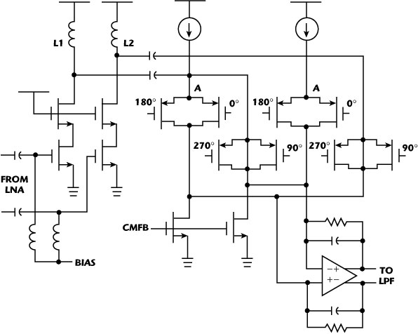
The pseudo differential low-noise amplifier (LNA) uses the nMOS common-source cascode topology with inductive source degeneration provided by the bonding wire to minimize the chip size. The LNA is switched to low gain mode to alleviate the linearity requirement on the following stages when a large RF input signal is present. To remove the DC-offset due to the LO self-mixing, the double-balanced sub-harmonic mixer shown in Figure 2 is used for quadrature down-conversion.

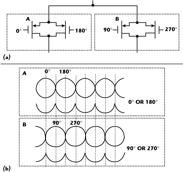
The LO frequency is half that of the RF input frequency and therefore, octa-phase LO signals, spaced by 45°, are required for quadrature down-conversion. As shown, the I-mixer uses 0°, 90°, 180°, and 270° LO signals while for Q-channel, 45°, 135°, 225°, and 315° LO signals are used. For sub-harmonic mixing, conventionally two stacked LO switching stages are used, which requires large voltage headroom5-6.
In this work, only one stack of switching stage is used to allow the low-voltage operation and the principle of harmonic mixing is illustrated in Figure 3. The switching stage is composed of pMOS transistors to minimize the flicker noise7-8. The output of the transconductance stage is AC-coupled to the switching stage to prevent the low-frequency even-order harmonics and DC-offset of the transconductance stage from being leaked to the mixer output.
An additional advantage of the AC-coupling is the independent biasing of the transconductance and switching stages, facilitating the design optimization such as conversion gain, noise figure, and linearity. The output current of the mixer is converted to voltage by an active-RC first-order filter whose cut-off frequency is tuned by the same code as the channel selection filter (CSF) following the mixer.
Analog Baseband
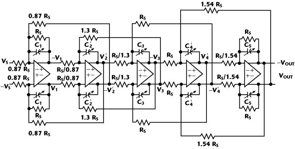
The analog baseband consists of I/Q signal paths, which include CSF, programmable gain amplifier (PGA), and DAC for DC-offset cancellation. At the input of the CSF, I- and Q-paths have separate DC-offset canceling R-2R ladder type DAC with 7-bit resolution as shown in Figure 4. The DC-offset canceling code is generated by a separate digital baseband modem.
For channel selection filtering, a fifth-order Chebyshev filter shown in Figure 5 is used because it provides a relatively large stop-band attenuation with moderate group delay variation within the pass-band. Between Gm-C and active-RC type implementation options, the active-RC type is adopted for its better linearity.
The dynamic range of the filter is maximized by scaling the resistor's values to have the same maximum signal swing for all internal nodes. The gain of the PGA (see Figure 6)can be controlled from 2.5 to 52.5 dB in 0.5 dB steps.
Because the operational amplifier (op-amp) for CSF and PGA should be able to provide virtual ground for out-of-band signals, the required bandwidth of the op-amp is much larger than the channel bandwidth. However, with a conventional frequency compensation method using a Miller capacitor, a large bandwidth can be obtained only with large power consumption. The op-amp used here employs a feedforward frequency compensation method shown in Figure 7, whose transfer function is given as
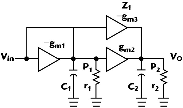

where


From Equations 1 and 2, the phase shift of the poles can be compensated with a left-half plane zero whose position can be varied by controlling A3. The op-amp, employing the feedforward frequency compensation scheme, is shown in Figure 8.

In order to reduce the current consumption, the differential pair (M6 and M7) generating gm3 is re-using the bias current of gm211. The simulation results, including all the parasitic capacitance, indicate 57.4 dB DC gain and 332 MHz unity gain frequency with 6 pF load capacitance as shown in Figure 9.
Octa-phase LO Generation
For quadrature down-conversion with sub-harmonic mixing, octa-phase local oscillator (LO) signals are required at half of the RF input frequency. A ring-type four-stage LC voltage-controlled oscillator (VCO), shown in Figure 10, is used for low phase noise.
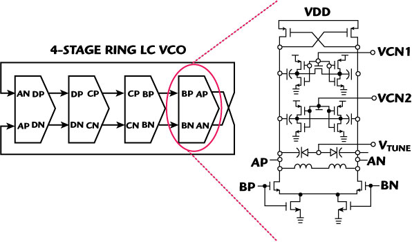
The switched tail current biasing scheme is applied, which is known to reduce the flicker noise of the biasing transistor by periodically releasing the trapped electrons 12-14. Two-bit digital inputs, VCN1 and VCN2, coarsely control the oscillation frequency with a capacitor bank.
The LC VCO is embedded in an integer-N type phase locked loop (PLL) as shown in Figure 11. The divide-by-N block of the PLL shown has a multi-modulus (16/17/18/19) prescaler, instead of the normally used dual-modulus one.
With a conventional dual-modulus prescaler, the counting ratio of an asynchronous programmable counter can be as large as 256, resulting in a large delay and the re-timing with the prescaler output becomes very difficult.
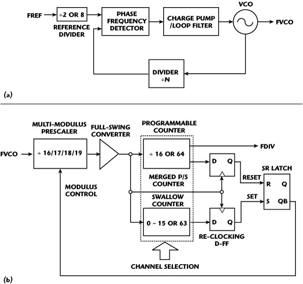
The programmable and swallow (P/S) counters are merged together to reduce the silicon area. The output of the merged P/S counter is re-timed by the output clock of the multi-modulus prescaler to reduce the jitter of the divided-by-N clock.
The loop filter of the PLL is implemented off-chip. The octa-phase outputs of the VCO are buffered by Cherry-Hooper type amplifiers to have sufficient voltage swing.
The phase noise of the open- and closed-loop octa-phase VCO is -120 dBc/Hz and -108 dBc/Hz, respectively, at 1 MHz offset, as shown in Figure 12. The phase error between the octa-phase LO signals is less than 1° over the whole frequency range.
Experimental Results
The 5 GHz direct-conversion receiver has been implemented in a 0.18 μm CMOS technology whose microphotograph is shown in Figure 13. The chip occupies a core area of 5.76 mm2 and is packaged in a 48-pin MLF package with exposed die.
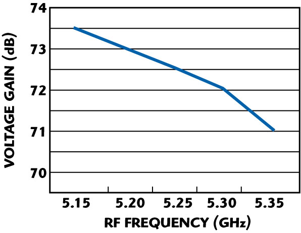
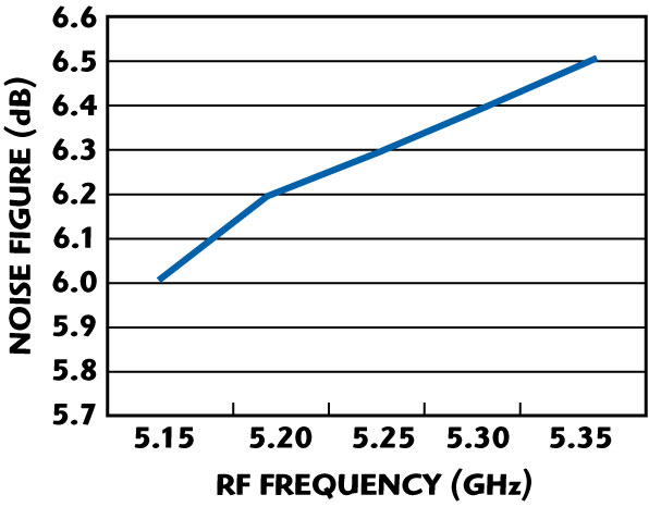
The measured voltage gain and noise figure of the overall receiver are 71.0 to 73.5 dB and 6.0 to 6.5 dB, as shown in Figures 14 and 15, respectively.
The third-order input intercept point (IIP3) is measured to be -4 and -16 dBm, respectively at the low- and high-gain modes of the LNA, as shown in Figure 16.
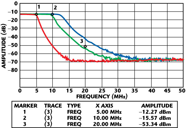
The cut-off frequency of the CSF can be controlled from 5 to 12.7 MHz as shown in Figure 17 and the stop-band rejection is greater than 40 dB.

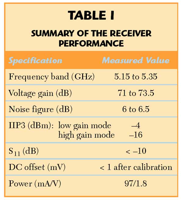
The gain error of PGA is less than 0.25 dB over the whole gain control range. The measured performance of the receiver is summarized in Table 1.
Conclusion
A direct-conversion receiver for 5 GHz wireless LAN has been developed. To minimize the DC-offset due to LO self-mixing, sub-harmonic mixing is used for the down-conversion.
For quadrature sub-harmonic mixing, octa-phase LO signals are generated by an integer-N type frequency synthesizer. Implemented in a 0.18 μm CMOS technology, the receiver dissipates 97 mA from a 1.8 V supply and has 6.5 dB NF and -4 dBm IIP3.
Acknowledgment
Part of this work was supported by the Center for Advanced Transceiver Systems (CATS), Seoul National University and HY-SDR Research Center, Hanyang University, Seoul, Korea, under the ITRC Program of MIC, Korea. The CAD tools were supported by IDEC.
References
1. J. Vassiliou, K. Vavelidis, T. Georgantas, S. Plevridis, N. Haralabidis, G. Kamoulakos, C. Kapnistis, S. Kavadias, Y. Kokolakis, P. Merakos, J. C. Rudell, A. Yamanaka, S. Bouras and I. Bouras, “A Single-chip Digitally Calibrated 5.12-5.825GHz, 0.18 μm CMOS Transceiver for 802.11a Wireless LAN,” IEEE Journal of Solid-State Circuits, Vol. 38, No. 12, December 2003, pp. 2221-2231.
2. P. Zhang, T. Nguyen, C. Lam, D. Gambetta, T. Soorapanth, B. Cheng, S. Hart, I. Sever, T. Bourdi, A. Tham and B. Razavi, “A 5GHz Direct Conversion CMOS Transceiver,” IEEE Journal of Solid-State Circuits, Vol. 38, No. 12, December 2003, pp. 2232-2238.

3. B. Razavi, “RF Microelectronics,” Prentice-Hall, Upper Saddle River, NJ, 1998.
4. IEEE Standard 802.11a-1999, Part 11: Wireless LAN Medium Access Control (MAC) and Physical Layer (PHY) Specifications.
5. L. E. Larson, “A Wide-bandwidth SiGe HBT Direct Conversion Sub-harmonic Mixer/Down-converter,” IEEE Journal of Solid-State Circuits, Vol. 35, No. 9, September 2000.
6. S. J. Fang, S. T. Lee and D. J. Allstot, “A 2 GHz CMOS Even Harmonic Mixer for Direct Conversion Receivers,” 2002 IEEE International Symposium on Circuits and Systems, Vol.4, pp. 807-810.
7. J. Chang, A. A. Abidi and C. R. Viswanathan, “Flicker Noise in CMOS Transistors from Subthreshold to Strong Inversion at Various Temperatures,” IEEE Transactions on Electron Devices, Vol. 41, No. 11, November 1994, pp. 1965-1971.
8. D. M. Binkley, J. M. Rochelle, B. K. Swanna, L. G. Clonts and R. N. Goble, “A Micropower CMOS Direct-conversion, VLF Receiver Chip for Magnetic-field Wireless Applications,” IEEE Journal of Solid-State Circuits, Vol. 33, No. 3, March 1998, pp. 344-358.
9. M.T Terrovitis and R. G. Meyer, “ Intermodulation Distortion in Current-commutating CMOS Mixers,” IEEE Journal of Solid-State Circuits, Vol. 35, October 2000, pp. 1461-1473.
10. H. Darabi and A. A. Abidi, “Noise in RF-CMOS Mixers: A Simple Physical Model,” IEEE Journal of Solid-State Circuits, Vol. 35, No. 1, January 2000, pp. 15-25.
11. J.-H. Hwang and C. Yoo, “A Low-power Wide-bandwidth Fully Differential Operational Amplifier with Current re-using Feedforward Frequency Compensation,” 2004 IEEE Asia-Pacific Conference on Advanced System Integrated Circuits Proceedings, pp. 32-35.
12. C.-Y. Jeong and C. Yoo, “5 GHz Low-phase Noise CMOS Quadrature VCO,” IEEE Microwave and Wireless Component Letters, Vol. 16, No. 11, November 2006, pp. 609-611.
13. C. C. Boon, M. A. Do, K. S. Yeo, J. G. Ma and X. L. Zhang, “RF CMOS Low-Phase-noise LC Oscillator Through Memory Reduction Tail Transistor,” IEEE Transactions on Circuits and Systems, Part II, Vol. 51, No. 2, February 2004, pp. 85-90.
14. E. A. M. Klumperink, S. L. J. Gierkink, A. P. van der Wel and B. Nauta, “Reducing MOSEF 1/f Noise and Power Consumption by Switched Biasing,” IEEE Journal of Solid-State Circuits, Vol. 35, No. 7, July 2000, pp. 994-1001.