
Introduction
Applying frequency modulation to a frequency synthesizer is a classic case of conflicting requirements. Great care is taken to design the synthesizer to make the output frequency as pure and stable as possible. The requirement for FM however, is to be able to perturb the frequency as much as possible. The result is that compromises must be made to both functions.
Since the primary requirement of a general purpose synthesized signal generator is spectral purity, most of the compromises are made to the FM function. Several innovative design techniques have been implemented in the Giga-tronics 2500 signal generator microwave synthesizer to enhance its frequency agility and FM capability without compromising its excellent spectral purity. This article discusses the methods used to frequency modulate the 2500 signal generator and the FM performance obtainable. After a brief review of angular modulation (FM and Phase Modulation) theory, the various modes available for FM in the 2500 signal generator and their advantages and limitations will be described in detail. Then suggestions are made for obtaining better than specified FM performance and several methods for characterizing FM performance are described.
The published specifications for complex instrument like the Giga-tronics 2500 signal generator can only partially describe its characteristics and attributes, but by fully understanding the design of the instrument, the user can better exploit its capabilities.
Review of Angular-Modulation
Let's start with a brief review of the principles of angular modulation. See appendix A for a detailed mathematical derivation of frequency- and phase-modulated signals.
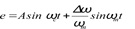
The general equation for an AC signal in the time domain is
e = A sin(ωt + θ) (1)
Where e is the instantaneous amplitude of the signal, A is the peak amplitude, ω is the instantaneous frequency1, t is time, and θ represents the phase at t = 0. Angular-modulation occurs when modulation is applied to the argument (the angle) of the sine function in Equation (1). Either the frequency, ωi or the phase, θ may be modulated.
Frequency-Modulation
A frequency-modulated signal is one whose instantaneous frequency, ωi is varied in accordance with the modulating signal. In the time domain, the equation for an FM signal is
e = A sin(ωct + Β sin ωmt) (2)
Where ωc is the angular velocity or frequency of the unmodulated or carrier wave, Β is the modulation index, and ωm is the modulating frequency or modulation rate.
The modulation index, Β is defined as the ratio of the maximum frequency deviation from the unmodulated carrier frequency to the frequency of the modulating signal,
 (3)
(3)
It is important to note that the modulation index Β has the units of radians and represents the maximum instantaneous phase deviation from the unmodulated carrier wave. It will be seen later that in some systems, this is a fundamental limitation of FM performance. Figure 1 shows a frequency-modulated signal (bottom trace) along with the modulating signal (top trace) for comparison. The deviation has been greatly exaggerated for clarity.

Figure 1. FM signal and the corresponding modulating signal.
A fundamental characteristic of a frequency-modulated signal is that the frequency deviation, Δω is proportional to the peak amplitude of the modulating signal, and is independent of the modulating frequency.
The frequency spectrum of an FM signal consists of an infinite number of sideband pairs on each side of the carrier spaced at multiples of the modulating frequency. The magnitude of the carrier and each pair of sidebands is related to the modulation index by Bessel functions of the first kind and order equal to the sideband number. For example, the carrier magnitude with respect to the unmodulated carrier is the zeroth order Bessel function and the magnitude of the first sideband pair is the first order Bessel function. Figure 2 shows how the first few Bessel functions vary with the modulation index and Figure 3 shows the relative level of the carrier and the first few sidebands with respect to the unmodulated carrier.
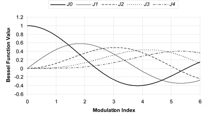
Figure 2. Bessel functions.
Note that for certain values of modulation index, the Bessel functions go through zero and the level of the carrier or corresponding sidebands goes through a null. This provides a convenient and accurate method of determining modulation index from which deviation can be determined accurately. For example, the carrier level goes to zero at a modulation index of 2.405 (the first Bessel null). If the modulation rate is 1 kHz, this corresponds to a deviation of 2.405 kHz.
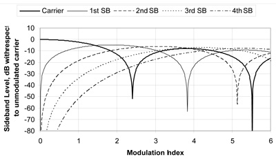
Figure 3. FM sideband levels vs. modulation index.
The foregoing description is based on a sinusoidal modulating waveform. For non-sinusoidal modulation, the frequency spectrum becomes very complicated. When both frequency- and amplitude-modulation are combined, either on purpose or due to errors in the system, the modulation sidebands are generally no longer symmetrical about the carrier.
Phase-Modulation
A phase-modulated signal is one in which the instantaneous phase θ in Equation (1) is varied in accordance with the modulating signal. The time domain equation for a phase-modulated signal is
e = A sin(ωt + δθsinωmt) (3)
Note the similarity of Equation (3) which describes phase-modulation to Equation (2), repeated here, which describes frequency-modulation.
e = A sin(ωt + Βsinωmt) (2)
In both cases, the modulation indices have the units of radians and represent the maximum instantaneous phase deviation from the unmodulated carrier wave. However, the phase modulation index, δθ is proportional to the peak amplitude of the modulating signal, and is independent of the modulating frequency while the frequency-modulation index, Β is proportional to the peak amplitude of the modulating signal and inversely proportional to the modulating frequency.
Effects of Frequency Multiplication, Division, and Translation
When a signal with angular-modulation is passed through a frequency multiplier or divider, the frequency or phase deviation is multiplied or divided by the same amount as the carrier but the modulating frequency or rate remains constant.
For example, if a 5 GHz signal that is frequency-modulated at a 10 kHz rate with 1 MHz deviation is passed through a frequency tripler, the resultant 15 GHz signal will have 3 MHz deviation but the modulation rate will still be 10 kHz. This has the effect of multiplying the modulation index by a factor of three. Likewise, a 5 GHz signal phase-modulated at a 10 kHz rate with a phase deviation of π radians will have a phase deviation of 3π radians after passing through a frequency tripler, multiplying its modulation index by three.
When a 4 GHz signal frequency-modulated with 1 MHz deviation at a 100 kHz rate is passed through a frequency divider with a division ratio of 8, the resultant 500 MHz signal is still modulated at the 100 kHz rate, but the deviation is reduced to 125 kHz, reducing the modulation index by a factor of eight.
Frequency translation (heterodyning) preserves the original modulation, so the frequency and phase deviation of the original signal is preserved in the translated signal.
FM in the Giga-tronics 2500 Signal Generator/ Microwave Synthesizer
Figure 4 is a simplified block diagram of the Giga-tronics 2500 signal generator showing how the FM system is integrated into the synthesizer. A YIG-tuned oscillator (YTO) covering the 4 to 10 GHz frequency range is phase locked to a low noise VHF variable frequency reference using Giga-tronics’ proprietary Accumulative High Frequency Feedback (AHFF) technology. The variable reference incorporates direct digital synthesis to vary its frequency in fine steps over a narrow range. The heart of the AHFF technology is a fractional divider designed to overcome the limitations of traditional fractional-N and sigma-delta systems2. Microwave frequency multipliers extend the YTO frequency up to 40 GHz, depending on the synthesizer model. Frequency dividers and filters generate output frequencies down to 10 MHz.
The modulating signal, either internally generated or applied to the external FM input on the instrument’s rear panel, is first processed by analog circuitry that buffers the signal and allows the user to set the deviation or FM sensitivity. For high modulating frequencies, the incoming FM signal is amplified and applied directly to the YTO. This mode, which supports deviations up to 20 MHz and modulating frequencies up to 3 MHz, is called wide-mode FM. For low modulating frequencies (including DC) and high modulation indices, the incoming FM signal is digitized and digitally summed with the tuning word for the DDS. Because the maximum modulating frequency is limited by the phase locked loop bandwidth to approximately 50 kHz, this mode is called narrow-mode FM.

Figure 4. Giga-tronics 2500 Synthesis and FM Block Diagram.
In addition to these two FM modes, provision is made to electrically tune the 100 MHz frequency reference over a limited range. While this is of limited use as an FM function, it does provide a true analog DC FM input which is useful for applications where the discontinuous analog response of an analog to digital converter cannot be tolerated.
Wide-mode FM
For high modulation rates, the analog FM signal is used to directly modulate the YTO via the “FM” or “tickler” coil.
The advantage of this method is that the upper modulation rate is limited only by the frequency response of the analog circuitry and the YTO’s FM coil. Wide mode frequency response in the 2500 signal generator is specified from 10 kHz to 5 MHz and maximum deviation is specified as 20 MHz, subject to the modulation index limit discussed below.
A drawback is that the lower limit of the modulation rate is limited by the phase locked loop bandwidth. At modulation rates within the loop bandwidth, the loop sees the FM as a frequency or phase error and tries to correct for it, effectively attenuating the modulation. To allow reasonably low modulating rates in the wide-band mode and a good overlap with the frequency response of the narrow-band mode, the bandwidth of the YTO phase locked loop is reduced from the normal bandwidth of approximately 70 kHz to about 5 kHz. As a result, the phase noise increases slightly when wideband FM is enabled.
Another drawback is that even well above the loop bandwidth, the modulation index is limited by the phase excursions the phase locked loop’s phase detector can handle. It will be recalled from frequency modulation theory that modulation index is the maximum phase excursion of the modulated signal. The phase/frequency detector used in the phase locked loop is limited to phase excursions on its inputs of ±2π radians (approximately 6.28 radians or 360 degrees) which corresponds to a modulation index of 2π at the phase detector’s input. With phase excursions greater than this, the phase detector’s output clips and the phase locked loop is no longer a linear feedback system. This occurs even when the modulation rate is outside the loop bandwidth. For this reason the maximum modulation index is specified as 15 for a carrier frequency of 4 GHz.
Narrow-mode FM
In the narrow FM mode, the modulating signal is digitized by a 10 bit, 20 mega sample/sec analog-to-digital converter. The ADC’s digital output is summed with the DDS tuning word to vary the DDS’s frequency in accordance with the modulation. This method has the advantage that it retains the frequency stability and low noise of the synthesizer and allows for modulation rates down to and including DC. Frequency response is very flat and distortion is low. The disadvantage is that the upper limit of the modulating frequency or rate is determined by the speed of the analog to digital converter, the maximum rate at which the DDS can be updated, and the bandwidth of the phase locked loop. In the 2500 signal generator, the narrow-band FM frequency response is DC to 50 kHz. There is no limit to the modulation index, but due to circuit constraints, deviation is limited to 1 MHz at the output of the YTO3.
The upper 3 dB limit of the modulation rate is primarily due to the anti-aliasing filters associated with the analog to digital converter and the phase locked loop’s bandwidth. The specification for the maximum narrow-band modulation rate is set at 50 kHz and the frequency response rolls off rapidly at higher frequencies.
The narrow-band mode provides a convenient way of linearly varying the synthesizer’s frequency with an analog DC voltage while retaining the instrument’s inherent frequency stability and low phase noise. Of course, any noise or variations in the tuning voltage are transferred directly to the synthesizer’s output so care must be taken to keep the tuning voltage clean. The voltage-to-frequency transfer function in this application is quite linear and well defined, but the finite 10-bit resolution of the analog-to-digital converter makes it discontinuous so it may not be suitable for applications which require the instrument's output frequency to be a continuous function of the control voltage.
Reference Tune
Some applications require phase locking the synthesizer to another stable microwave source. One such application would be to compare the phase noise the other source with that of the Giga-tronics 2500 signal generator. For these types of applications where truly continuous control over the synthesizer's frequency is required, a DC voltage can be used to tune the internal 100 MHz reference oscillator over a limited range. This oscillator is an oven-controlled low noise crystal oscillator (OCXO) that is normally phase-locked to either a high stability 10 MHz OCXO or an external reference signal. When the Reference Tune input is enabled, the 100 MHz OCXO is directly controlled by a tuning voltage applied to the rear panel. Unlike the narrow-band FM mode, this is a truly continuous analog control with infinite resolution. The tuning range at 100 MHz is approximately ±600 Hz for a tune voltage range of 0.5 volts to 10 volts. When referred to the synthesizer’s output frequency, the tuning range is scaled directly. For example, the tuning range is approximately ±30 kHz at 5 GHz4 but only approximately ±300 Hz at 50 MHz. When driven by a voltage source, the frequency response is typically 3 dB down at 1 kHz5.
Pushing FM Performance Beyond the Specs
Wide-mode FM
Table 1 lists the specifications for wide mode FM in the Giga-tronics 2500 signal generator.
Giga-tronics 2500 signal generator Wide-mode FM Specifications
Frequency Response (3 dB bandwidth) | 10 kHz to 5 MHz |
Maximum Deviation | 20 MHz* |
Maximum Modulation Index (carrier = 4 GHz) | 15* |
* Maximum deviation is limited to 20 MHz or a modulation index of 15, whichever is greater. | |
As explained above, the modulation index is limited by the phase excursions that can be handled by the phase lock loop phase detector. The fractional frequency divider between the YTO and the input to the phase detector, shown in Figure 4, divides the modulation index or phase excursions so that at the YTO’s output frequency, the limit of 2π radians imposed by the phase detector is increased by the divide number. The divide number ranges from approximately 5.9 when the YTO’s output frequency is 4 GHz to approximately 14.7 for a YTO frequency of 10 GHz. Thus the theoretical allowable modulation index at the YTO’s output ranges from approximately 11.8π (β=37) to approximately 29.4π (β=92). However, once the phase detector’s limit has been exceeded, the modulation index must be reduced to below half that value for the phase detector to re-enter its linear region and the loop to recover6. Experience has shown that the modulation index should be limited to slightly less than this to allow phase errors in the system to be accommodated. Although the modulation index limit is greater at higher YTO frequencies, the instrument’s specification has been conservatively set at 15.
Measurements made on an actual instrument with a variety of modulation rates verify that at a YTO frequency of 4 GHz, the phase locked loop always remains locked for a modulation index up to about 18. When the YTO frequency is 10 GHz, the loop remains locked for a modulation index up to about 45. The modulation index limit is proportional to YTO frequency and Table 2 shows values for several YTO frequencies between 4 GHz and 10 GHz. It is usually possible to increase the modulation index beyond these values, but once the phase detector’s range is exceeded, modulation index will have to be reduced to the value listed in the table for the loop to properly recover.
Table 2. Maximum Useful Modulation Index in Wide Mode.
YTO Frequency | Maximum Useful Modulation Index |
4 GHz | 15 |
5 GHz | 18 |
6 GHz | 22 |
7 GHz | 26 |
8 GHz | 30 |
9 GHz | 34 |
10 GHz | 37 |
Note that the values of modulation index listed in Table 2 as well as the maximum deviation listed in Table 1 are for the fundamental output frequency of the YTO, band 10 as listed in Table 3. For other instrument output frequencies, both the modulation index and the maximum deviation are divided by the number N listed in Table 3.
Table 3. Giga-tronics 2500 signal generator Output Bands
Band | Frequency | N |
0 | 0.1– 9.99 MHz | N/A |
1 | 10 –<15.625 MHz | 512 |
2 | 15.625 – <31.25 MHz | 256 |
3 | 31.25 – <62.5 MHz | 128 |
4 | 62.5 – <125 MHz | 64 |
5 | 125 – <250 MHz | 32 |
6 | 250 – <500 MHz | 16 |
7 | 500 – <1000 MHz | 8 |
8 | 1.0 – <2.0 GHz | 4 |
9 | 2.0 – <4.0 GHz | 2 |
10 | 4.0 – <10.000 000 1 GHz | 1 |
11 | 10.000 000 1 – <20.2 GHz | 1/2 |
12 | 20.2 – 40.0 GHz | 1/4 |
Combining the modulation index limit as a function of carrier frequency listed in Table 2 with the division ratios listed in Table 3, it can be seen that the modulation index limit is proportional to carrier frequency across the entire output frequency range of the instrument and can be expressed as 3.75 times the carrier frequency in GHz.
When the modulation index limit is exceeded, the phase locked loop is driven out of its linear operating region. If the synthesizer's output is viewed on a spectrum analyzer, the overall frequency spectrum doesn’t appear to change significantly, but in this condition the phase detector is behaving as a frequency detector and the YTO’s output is no longer phase coherent with the loop’s reference frequency. Phase noise increases and the YTO frequency shifts slightly, depending on how far the phase detector is over driven. These effects vary not only with modulation index, but also with the modulating frequency and are not predictable. In addition, the modulating waveform becomes distorted due to the phase detector’s non-linear response.
In wide mode, maximum FM deviation is 20 MHz at the YTO fundamental frequency (the 4 - 10 GHz band). In other bands, the maximum deviation is 20 MHz divided by the number N for each band listed in Table 3. At 100 MHz, the maximum deviation is 20 MHz/64 or 312 kHz and at 26 GHz, the maximum deviation is 20 MHz/0.25 or 80 MHz. Note that for carrier frequencies close to the band edges, it is possible to double the maximum deviation (as long as the modulation index limit is not exceeded) simply by choosing a frequency on the high side of the band crossing. For example if an X-band device is being tested with an FM rate of 1 MHz, it is possible to obtain only 20 MHz deviation at 9.5 GHz, but 40 MHz deviation can be obtained at 11 GHz. However, the phase noise of the carrier will also increase each time a higher band is selected.
FM sensitivity is calibrated in terms of deviation per volt peak, i.e., a signal level of 0.5 volts peak will result in 500 kHz deviation when the FM sensitivity is set to 1 MHz/volt. The maximum input voltage to the instrument's external FM input is 1 volt peak (0.707 volts RMS for a sine wave input) so the maximum deviation is obtainable only with the 20 MHz/volt sensitivity setting.
Figure 5 shows measured deviation versus modulating frequency for various FM sensitivities at a carrier frequency of 7 GHz. At this carrier frequency, the modulation index is limited to 3.75*7 or about 26. Note how the modulation index limits the deviation at low modulation rates. For example, at this carrier frequency 20 MHz deviation can only be achieved at modulating frequencies above 770 kHz. The deviations and modulation index limits shown in Figure 5 are scaled for other bands by the number N listed in Table 3.
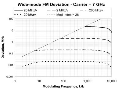
Figure 5. Wide-mode deviation as a function of modulating frequency.
The 3 dB bandwidths for the FM sensitivities shown in Figure 5 can be inferred from the figure by noting that -3 dB is a ratio of 0.707. Thus the 3 dB bandwidths correspond to the points where the deviation has fallen to 0.707 of the mid-band value. Since the mid-band values plotted in Figure 5 are decade multiples of 2.0, their corresponding -3 dB points are decade multiples of 1.414. On the instrument that was measured, the 3 dB bandwidth of the 20 kHz/volt setting is from 4 kHz to about 5.6 MHz.
Narrow-mode FM
Figure 6 shows measured deviation as a function of modulating frequency for various sensitivities in the narrow mode. Although the frequency response extends all the way down to DC, the lower limit of the instruments used to make this measurement was 5 Hz.

Figure 6. Narrow-mode deviation as a function of modulating frequency.
At the YTO's fundamental frequency (4-10 GHz, corresponding to N=1 in Table 3) the maximum deviation in narrow-mode is 1 MHz, but there is no limitation on the modulation index. As with wide-mode, the maximum deviation is divided by the number N listed in Table 3. At 100 MHz, N = 64 and the maximum deviation is 15.625 kHz; at 26 GHz, N = 0.25 and the maximum deviation is 4 MHz. Again, for applications with carrier frequencies close to the band edges, deviation can be maximized by choosing a carrier frequency on the high side of the band crossing.
The narrow-mode 3 dB bandwidth can be inferred from Figure 6 in the same way the wide-mode bandwidth was determined from Figure 5. For this particular instrument, the 3 dB bandwidth ranged from 55 kHz in the 1 kHz/volt sensitivity setting to about 63 kHz in the 1 MHz/volt setting.
Noise
In wide-mode, the synthesizer's phase locked loop bandwidth is reduced to allow the FM frequency response to extend down to 10 kHz. This has the side effect of increasing the carrier's phase noise when wide-mode FM is enabled. However, in applications using FM the signal to noise ratio of interest is the ratio of FM deviation due to the modulating signal to deviation caused by residual FM7 with no modulation applied. This is also the signal to noise ratio of the FM signal after it has been demodulated by a noiseless discriminator.
Using the maximum possible deviation consistent with the application at hand ensures the maximum signal to noise ratio. Signal to noise ratio is also maximized by using the maximum possible analog input to the FM system and adjusting deviation by adjusting the instrument’s FM sensitivity setting.
The same consideration also applies to the narrow-mode. Although the phase locked loop is operating at its normal bandwidth, phase noise is slightly degraded in the narrow-mode due to the added noise of the analog FM circuitry ahead of the analog to digital converter. In addition, using the max possible analog input in narrow-mode and adjusting deviation with FM sensitivity setting maximizes the effect of the finite resolution of the 10 bit A/D converter.
Characterizing FM Performance
Characterizing the performance of an FM system usually involves measuring the FM sensitivity versus modulating frequency for a sinusoidal modulating signal. FM sensitivity is determined by measuring the deviation resulting from a modulating signal of known amplitude. Deviation can be measured in several ways, such as the use of a spectrum analyzer to observe Bessel nulls, demodulating the FM signal with a calibrated discriminator or using one of the commercially available measuring receivers.
Bessel Nulls
We have seen that the level of the carrier and each sideband is described by the corresponding Bessel function. Perhaps the simplest and most accurate method of measuring the deviation of a sinusoidally modulated signal is to set the modulation index to a value that results in a null of the carrier or one of the sidebands. For example, we know that at a modulation index of 2.405, the carrier level goes to zero. If the modulating frequency is 50 kHz, the deviation is easily calculated to be 2.405 times 50 kHz or 120.25 kHz. Conversely, if it is desired to set a certain deviation, it is easy to calculate the modulating frequency that will yield a Bessel null at the desired deviation.
The following table lists values of modulation index for which the carrier and the first few sidebands go to zero.
Modulation Indices for Bessel Nulls
Null | 1st | 2nd | 3rd | 4th | 5th | 6th |
Carrier | 2.405 | 5.520 | 8.654 | 11.792 | 14.931 | 18.071 |
1st Sideband | 3.832 | 7.016 | 10.173 | 13.324 | 16.471 | 19.616 |
2nd Sideband | 5.136 | 8.417 | 11.620 | 14.796 | 17.960 | 21.117 |
3rd Sideband | 6.380 | 9.761 | 13.015 | 16.223 | 19.409 | |
4th Sideband | 7.588 | 11.065 | 14.373 | 17.616 | 20.827 | |
5th Sideband | 8.771 | 12.339 | 15.700 | 18.980 | 22.218 |
Above the 6th carrier null, the carrier nulls repeat at intervals very close to π. That is, for the nth carrier null, β = 18.07+(n-6)π. By judicious use of carrier and sideband nulls it’s usually possible to measure the system’s frequency response at a sufficient number of points to plot a smooth curve.
For small values of modulation index, the first order Bessel function describing the first sideband approximately one half the modulation index or β/2. Thus measuring the level of the first sideband is a convenient way of determining low values of modulation index. For example, if the first sideband is 25 dB below the carrier, the modulation index is very close to 0.118. Up to a modulation index of 0.2 the error is less than 0.5% and it is less than 5% up to a modulation index of 0.5.
Delay Line Discriminator
For large modulation indices such as the case when the modulation rate is low compared to the deviation, and for small modulation indices where the deviation is low compared to the modulation rate, the method of using Bessel nulls to determine deviation becomes impractical. Also, making a continuous swept measurement of deviation versus modulating frequency is not possible using Bessel nulls. In these cases an FM discriminator may be used to recover the modulation in order to compare it to the original modulating signal.
The output of the ideal discriminator should be independent of amplitude variations in the input signal, and it should faithfully reproduce the modulating waveform at all modulation rates of interest. A simple but good performing discriminator for VHF and microwave frequencies is the delay line discriminator shown in Figure 7. See appendix B for a detailed analysis of its performance.

Figure 7. Delay line discriminator.
The delay line discriminator is easy to build and has good sensitivity and frequency response. It’s output is not independent of amplitude variations in the input signal, but this is usually not a problem when the peak to peak deviation is much less than the carrier frequency, and the system is well matched to avoid rapidly varying mismatch losses.
The length of the delay line is chosen to be an odd multiple of a quarter wavelengths at the carrier frequency. This makes the discriminator’s output zero for a carrier with no modulation. Changing the carrier frequency slightly makes the output go positive or negative depending on the direction of frequency change and which multiple of an odd quarter wavelength is used (see appendix B). Making the delay line long increases the sensitivity of the detector, but making it too long will result in distortion for large deviations. See appendix B for more detail on choosing the appropriate length. For carrier frequencies in the range of 5 to 10 GHz, and deviation up to a couple of megahertz, a few feet of 0.141 inch semi-rigid coax is a convenient choice. Rather than try to precisely trim the delay line length for a specific frequency, the carrier frequency is usually varied with no modulation until the discriminator’s DC output is zero. For applications where the carrier frequency is fixed and cannot be varied, a phase shifter can be added to one side or the other of the mixer to set the discriminator’s output to zero at the carrier frequency.
A typical passive double-balanced mixer requires about +7 to +17 dBm at it’s LO port, so the RF input needs to be about +10 to +20 dBm or higher. A fixed attenuator can be added to the delay line to reduce the power to the mixer's RF port to an appropriate level and foe better VSWR. The recovered modulation at the discriminator’s output depends on the delay line length and the deviation of the FM signal and is typically about a tenth of a volt for a few megahertz deviation. The signal to noise ratio is good though and the low output level is usually not a problem, especially if a tuned measuring receiver such as a vector network analyzer or spectrum analyzer is used to measure the recovered FM.
A carefully constructed delay line discriminator will have good frequency response for modulating rates up to several 10’s of megahertz. Its frequency response and sensitivity can be calibrated at several spot frequencies using Bessel nulls as described in the previous section. A DC calibration is easily made by simply shifting the unmodulated carrier slightly and noting the shift in the discriminator’s DC output.
Modulation Analyzers
Modulation analyzers such as the Hewlett-Packard (now Agilent Technologies) 8901A9 measure and display FM deviation directly. Some even provide an output for the demodulated signal that can be used for further analysis. However, the deviation and modulation rates they can handle are often limited to a few hundred kilohertz.
Swept Frequency Measurements
There are several ways of making swept frequency measurements of FM frequency response using a discriminator or modulation analyzer. Perhaps the simplest method is to vary the modulation rate with a manually tuned audio oscillator and observe the discriminator’s output with an oscilloscope or low frequency spectrum analyzer. If the spectrum analyzer has a tracking generator output, that can be used as the modulation source for a simple swept measurement. Another good choice is to use a low frequency vector network analyzer such as the HP 3577A or Agilent 4395A Combination Network/Spectrum/Impedance Analyzer.
Figure 8 shows a test setup for making swept frequency measurements of FM frequency response at constant deviation using a low frequency vector network analyzer. The network analyzer's source provides the modulating signal for the instrument under test and the R channel measures the modulating signal's amplitude via a two-resistor power divider10. If the network analyzer has high impedance inputs, a simple frequency compensated voltage divider can be used instead of the power divider as shown in Figure 9. The B channel measures the output of the discriminator and the ratio of B/R is displayed on the network analyzer. Depending on the desired drive level to the instrument's FM input, an attenuator may be needed to prevent the R channel from overloading. The frequency response of the power divider and attenuator, if used, can be removed by connecting the power divider's output directly to the B channel input and doing a normalization calibration on the network analyzer.

Figure 8. Measuring FM frequency response. Constant deviation method.
When measuring small deviations, the output of a delay line discriminator with practical line lengths can be very small (on the order of a few 10’s of microvolt) and the measurement can be contaminated by the modulating signal leaking around the instrument under test and the discriminator via ground loops. This can show up as errors in the frequency response measurement caused by the leakage signal adding in and out of phase with the signal of interest or as a high “measurement floor” when the leakage is significantly higher than the desired signal. High frequency leakage can sometimes be reduced by the use of common mode chokes on the instrument’s FM input and the discriminator output. Low frequency leakage can be reduced or eliminated by breaking ground loop paths with isolation transformers or a DC block in the RF path between the instrument under test and the discriminator. To be effective, the DC block must break both the inner and the outer conductors of the RF cable. Figure 9 shows the setup used to make the deviation measurements in Figure 5.

Figure 9. Common mode chokes and DC block used to measure low deviation FM frequency response.
Appendix A
Angular-Modulation
A complete treatment of frequency- and phase-modulation can be found in any good general electrical engineering textbook. This approach follows that of Terman11.
The general equation for an AC signal in the time domain is
e = A sin Φ(t) (A1)
Where e is the instantaneous amplitude of the signal, A is the peak amplitude and Φ(t) is the total angular displacement of the phase at time t. Angular-modulation occurs when modulation is applied to the argument of the sine function, Φ(t). The instantaneous angular frequency, ωi is the time derivative of the phase12,
 (A2)
(A2)
A constant-frequency sinusoidal signal is a special case of Equation (A2) where ωi is constant. Then,
 (A3)
(A3)
Where the constant of integration, θ represents the phase at t = 0. Substituting Equation (A3) into Equation (A1) yields the time domain equation for a sinusoidal signal:
e = A sin(ωit + θ) (A4)
Angular-modulation occurs when modulation is applied to the argument (the angle) of the sine function in Equation (A4). Either the frequency, ωi or the phase, θ may be modulated.
Frequency-Modulation
A frequency-modulated signal with sinusoidal modulation is one whose instantaneous frequency, ωi is varied according to13
ωi = ωc + Δω cos ωmt (A5)
Where ωc is the angular velocity or frequency of the unmodulated or carrier wave, Δω is the maximum instantaneous deviation from the carrier wave frequency, and ωm is the modulating frequency or modulation rate in radians/second.
A fundamental characteristic of a frequency-modulated signal is that the frequency deviation, Δω is proportional to the peak amplitude of the modulating signal, and is independent of the modulating frequency.
Combining Equations (A2) and (A5) and integrating with respect to time, the phase function Φ(t) is
 (A6)
(A6)
Where Φ the constant of integration θ is the angular position at t = 0. Setting θ equal to zero for convenience and substituting Equation (A6) into Equation (1) results in the equation of a frequency-modulated signal in the time domain:
 (A7)
(A7)
The ratio of peak deviation, Δω to the modulating frequency ƒm is called the modulation index, β:
(A8)
Where Δƒ and ƒm are the peak deviation and modulation rate, both in units of Hertz. Substituting Equation (A8) into Equation (A7) gives the equation for the frequency-modulated signal in terms of modulation index:
e = A sin(ωct + β sin ωmt) (A9)
It is important to note that the modulation index β has the units of radians and represents the maximum instantaneous phase deviation from the unmodulated carrier wave. In some instances, this is a potential limitation of FM performance.
The frequency components making up the spectrum of the FM signal represented by Equation (A9) can be found by expanding the right-hand side of the equation by the trigonometric formula for the sum of two angles and evaluating the resulting expression, This yields,
 (A10)
(A10)
Where Jn(β) is the Bessel function of the first kind and nth order with argument β.
From Equation (A10) it can be seen that the frequency spectrum of an FM signal consists of an infinite number of sideband pairs on each side of the carrier spaced at multiples of the modulating frequency. The magnitude of the carrier and each pair of sidebands is given by Bessel functions of the modulation index.
It should be remembered that the foregoing derivation is based on a sinusoidal modulating waveform. For non-sinusoidal modulation, the frequency spectrum becomes very complicated.
Phase-Modulation
A phase-modulated signal is a sine wave as represented in Equation (A4) where the phase, θ is varied with the modulating signal. Thus for a sinusoidal modulating signal at frequency ωm we have,
θ = θ0 + Δθ sin ωmt (A11)
Where θ0 is the phase in the absence of modulation and Δθ is the peak phase change caused by the modulating signal, and is called the phase modulation index. Equation (A11) implies that the modulating voltage varies in accordance with sin(ωmt). Note that this is 90 degrees different than the case of Equation (A5) which was used to develop frequency-modulation.
Substituting Equation (A11) into Equation (A4) and setting θ0 = 0 for convenience14 yields the equation for a phase-modulated signal in the time domain:
e = A sin(ωct + Δθ sin ωmt) (A12)
Note the similarity of Equation (A12) which describes phase-modulation to Equation (A9), repeated here, which describes frequency-modulation.
e = A sin(ωct + β sin ωmt) (A9)
In both cases, the modulation indices have the units of radians and represent the maximum instantaneous phase deviation from the unmodulated carrier wave. However, the phase modulation index, Δθ is proportional to the peak amplitude of the modulating signal, and is independent of the modulating frequency while the frequency-modulation index, &beta is proportional to the peak amplitude of the modulating signal and inversely proportional to the modulating frequency.
Appendix B
The Delay-Line Discriminator
The delay line discriminator consists of an analog multiplier (a mixer) with the two inputs derived from the FM signal being demodulated. One input is delayed in time from the other by an amount corresponding to a carrier phase shift of an odd multiple of π/2 radians. This delay is easily accomplished by a transmission line of length equal to an odd multiple of quarter wavelengths at the carrier frequency15. Figure B-1 shows a typical delay-line discriminator setup. A power divider supplies the two paths to the mixer and an attenuator reduces the signal to the mixer's RF port for better linearity. A low pass filter removes the carrier while retaining the demodulated output. Following is the mathematical analysis showing how the modulating signal is recovered from the frequency-modulated carrier.

Figure B-1. The delay-line discriminator.
In the time domain, the frequency modulated RF input is
 (B1)
(B1)
Where A is the amplitude and ωi is the instantaneous frequency of the FM signal. For an arbitrary modulating waveform ƒ(t), the instantaneous frequency is
ωi = ωc + Δω • ƒ(t) (See appendix A) (B2)
The input to the mixer via the delay line is
B sin (ωit + Φ) (B3)
Where B is the amplitude after dividing losses and the loss of the delay line and Φ is the phase shift due to the delay line. This phase shift is a function of frequency ωi, the delay line length L, and the propagation velocity in the line vp:
 (B4)
(B4)
The other input to the mixer, directly from the power divider is
C sin(ωit) (B5)
Where C is the amplitude after the loss of the power divider. The mixer output, Vo is the product of its two input voltages,
Vo = B sin(ωit + Φ) • C sin(ωit)
Recalling the trigonometric identity for the product of two sines,
sin x sin y = ½[cos(x - y) - cos(x + y)]
and letting x = ωit + Φ and y = ωit, the mixer output voltage becomes
Vo = ½BC[cos Φ - cos(2ωit + Φ)] (B6)
The first term is proportional only to the phase shift Φ through the delay line and the second term is a signal at twice the carrier frequency. The low pass filter after the mixer removes this term leaving
Vo = k cos Φ (B7)
Where k is a constant replacing the term 1⁄2BC.
The phase Φ in terms of the carrier frequency and modulation is found by substituting Equation (B2) into Equation (B4):
 (B8)
(B8)
But the delay line length, L has been chosen to be an odd quarter wavelength at the carrier frequency ωc, so the first term is always  radians16. Substituting Equation (B8) into Equation (B7) yields
 (B9)
(B9)
Recalling the trigonometric identity for the cosine of the sum of angles,

and letting the mixer output voltage, Vo reduces to
 (B10)
(B10)
Where the sign depends on which odd multiple of a quarter wavelength is chosen for the delay line. If the peak deviation is small enough to cause less that about a tenth radian phase shift through the delay line, the approximation that the sine function is equal to its argument is valid and the output voltage Vo is
 (B11)
(B11)
Thus the discriminator’s output voltage is directly proportional to the modulating function in Equation (B2) and faithfully reproduces the modulating signal. The quantity k(L/vp) in Equation (B11) is the gain constant for the discriminator. Note that the gain is proportional to the delay line length, L and is greater for long delay lines17.
As noted above, for the approximation sin x = x to hold true, the phase shift due to the delay line should be less than a tenth of a radian at peak deviation, Δω. Phase shift in a transmission line is 2π radians (360 degrees) per wavelength, so the delay line length L must be less than L< λ where λ is the wavelength at Δω. The wavelength of Δω in the delay line is,
λ = 
Where vp is the propagation velocity in the delay line, so the maximum delay line length is
 (B12)
(B12)
Where Δω is in units of radians per second and Δƒ is in units of Hertz. A few examples will illustrate the limitations of delay line length for faithful reproduction of the of the modulating waveform by the discriminator.
Example 1. What is the maximum delay line length for a deviation of 20 MHz?
A convenient delay line material is 0.141 inch semi-rigid coax which has a relative propagation velocity of 0.7. The delay line length is then,

Example 2. What is the maximum deviation that can be faithfully reproduced using a delay line of 5 feet (1.52 meters) of 0.141 inch semi-rigid coax?
Solving Equation B12 in terms of Δƒ,

For a given delay line length, the discriminator’s operating frequencies, i.e. the carrier frequencies at which the DC output will be zero, can be determined by calculating the frequency for which this length equals a quarter wavelength:
 (B13)
(B13)
The operating frequencies are then odd multiples of this frequency. With the delay line length of 0.167 meters as calculated in Example 1 above, the operating frequencies are:

Where n is an odd number. So the operating frequencies are approximately 314 MHz, 943 MHz, 1572 MHz, etc. The mixer and power divider must be suitably chosen for the desired operating frequency.
Footnotes
1. For simplicity in dealing with trigonometric functions, frequency is expressed as ω in units of radians/second. This analysis is equally valid when frequency is expressed as ƒ in units of Hertz where ω = 2πƒ.
2. J. Regazzi and R. Gill, “Signal Generator Melds Speed with Low Phase Noise”, Microwaves & RF, October 2006, pp. 103-108.
3. When an FM signal is passed through a frequency multiplier or divider, deviation and modulation index are also multiplied or divided accordingly. For simplicity, unless otherwise noted, deviation and modulation index are referred to the YTO’s fundamental frequency, the 4 – 10 GHz band.
4. The scaling factor is very close to the ratio of the synthesizer’s output frequency to 100 MHz. The exact relation is more complex and beyond the scope of this paper.
5. The frequency response is primarily determined by a single pole consisting of 150 ohms and 1 uF. The frequency of this pole will be lowered by any additional resistance in the driving source.
6. The explanation for this is beyond the scope of this paper, but can be inferred by studying the phase to voltage transfer function shown in the data sheets and applications information on any of the commonly available digital phase-frequency detectors.
7. Residual FM is given by equation RMS_Freq 
8. Sideband level ≈ 20Log(&betta;/2). Therefore first sidebands 25 dB below the carrier correspond to β ≈ 0.11.
9. Unfortunately, the HP 8901A Modulation Analyzer has been discontinued with no direct replacement.
10. When properly terminated, a two-resistor power divider holds the ratio of its two outputs constant. Thus the R channel input is a true representation of the input level to the instrument under test. The values of the two resistors must be the same and equal to the input impedance of the R channel and the instrument under test. See Russell A. Johnson, “Understanding Microwave Power Splitters”, Microwave Journal, December 1975.
11. Terman, Frederick Emmons, Electronic and Radio Engineering, McGraw-Hill, 1955, pp. 586-596.
12. For simplicity in dealing with trigonometric functions, frequency is expressed as ω in units of radians/second. This analysis is equally valid when frequency is expressed as ƒ in units of Hertz where ω = 2πƒ.
13. This assumes that the instantaneous value of the “sinusoidal” modulating voltage varies as cos(ωmt). This assumption results in no loss of generality, as the only difference between the sine and cosine functions is a 90 degree phase shift.
14. Setting θ0 = 0 causes no loss of generality, as θ0 is simply an constant phase offset of the carrier.
15. In actual practice, the connection between the power divider and mixer has finite length, so it’s the difference between this and the total delay line length that must equal an odd multiple of quarter wavelengths.
16. The delay-line length is nλ/4 where n = 1, 3, 5, 7, 9, etc. This corresponds to phase shifts of π/2, 3π/2, 5π/2, 7π/2, 9π/2, etc. Normalized to a full circle (2π radians or 360 degrees), the phase shift is either +π/2 or –π/2.
17. Note also that k as defined in Equation (B7) is a function of the input voltages to the mixer. This means the discriminator’s output voltage is dependent on the amplitude of the RF input signal as well as the instantaneous frequency. For this reason, the input signal level must be held constant and not allowed to vary with modulation.