
 The search for more efficient power amplifier technologies to address needs of the 3G and 4G base station market is a continuous one. Put simply, the efficiency of a power amplifier can be thought of as the amount of RF power it transmits divided by the amount of DC power it consumes in order to generate the RF signal. The difference between consumed DC and transmitted RF power is left as the waste product enemy of all things electronic—heat. Heat must be removed, so large and heavy heatsinks are used in base station superstructures, cooling fans run continuously and air conditioning systems strain to keep up with the thermal load.
Operators of GSM-based systems were accustomed to the high efficiencies of a saturated power amplifier design, so the 10 percent efficiencies of early 3G power amplifier products were a rude awakening, and they had the electric bills to prove it. In response, base station OEMs have been working to optimize their designs and have turned towards techniques such as digital pre-distortion and advanced circuit topologies to help improve the state-of-the-art in power amplifier efficiency.
Semiconductor device designers have also been hard at work to make advances in realized power efficiencies within power amplifier transistors. This combination of better semiconductor devices and more sophisticated amplifier designs have today produced power amplifiers that are on the order of 30 percent efficient—a lot better than the early days of 3G deployments, but still not where system operators want efficiency to be. For example: one major system operator has set a goal of 50 percent overall amplifier efficiency for its 3G system; now base station OEMs and RF power device providers are scrambling to find ways to meet this challenge. With 4G deployments and their more difficult signal environments looming on the immediate horizon, it is clear that some revolutionary new design techniques and device technologies will be needed to satisfy operator and radio manufacturer expectations.
LDMOS has an established reputation for handling linear signal amplification needs in base station applications where 30 percent overall PA efficiency is considered today’s state-of-the-art. Contrast this to the handset market, where GaAs amplifiers are the norm due to the much higher power-added efficiency (PAE) of GaAs. With handset battery life a crucial consideration, GaAs HBT has dominated the landscape. Could a high voltage GaAs process be developed that would allow similar efficiency gains to be realized in a linear base station application?
As a major GaAs, SAW and BAW manufacturer, as well as a lead researcher for a multi-year GaN development process through DARPA, TriQuint Semiconductor had a wealth of experience in high efficiency product development, design and manufacturing from which to address the need for a high voltage, high efficiency power amplifier for 3G and 4G base stations. TriQuint compared the capability of GaAs and GaN processes in terms of performance, ruggedness and cost structure, and selected its proprietary InGaP GaAs High Voltage HBT (HV-HBT) technology as the best option for improving the efficiency of 3G and 4G power amplifier applications.
TriQuint had previously announced results of its HV-HBT process technology research in the form of efficient but relatively low power transistors for the base station market. More recently, the company has worked to improve the semiconductor processes, device designs and assembly steps needed to realize a new generation of even higher performance devices with correspondingly higher power levels. Results demonstrated by preproduction devices show the most recent design iterations to be extremely well suited for use in advanced circuit topologies being implemented by base station OEMs, which will in turn help drive the next leap forward in 3G and 4G base station amplifier efficiencies.
The initial device created to demonstrate the capabilities of the process was designated TGH2932-FL. Housed in an industry-standard ceramic package, it was designed as a 140 W peak power device optimized for the 2110 to 2170 MHz WCDMA band. In a typical one-carrier WCDMA signal environment that exhibits 7.4 dB PAR (peak-to-average ratio) at 0.01 percent CCDF (complementary cumulative distribution function), the TGH2932-FL delivers 25 W of average power with 14.5 dB of gain and a collector efficiency of 34 percent. The TGH2932-FL is highly pre-distortable, exhibiting low memory effects, and well-behaved AM-AM and AM-PM characteristics.
Using commercially available digital pre-distortion correction and crest-factor reductions, adjacent channel power products in this stimulus case are better than –60 dBc. The collector efficiency of 34 percent is impressive by itself, but when the TGH2932-FL is used in a Doherty amplifier configuration, the performance truly excels. In a Doherty amplifier, two devices are used together to form a single amplifier output stage. One of the devices is used as the main amplifier, biased in a conventional class AB mode. The second device is used as a peaking amplifier, and is biased towards class C operation. Since 3G and 4G signals have a very high PAR, the peaking amplifier is available to deliver power during those instantaneous peaks, but is turned off (consuming no DC power) when the signal peaks are absent. Because the peaking amplifier handles the peak power demands, the main amplifier can be operated much closer to compression; at this point collector efficiency climbs markedly.
Additionally, the two devices in a Doherty configuration (main and peaking) are combined in such a way that the main amplifier “sees” different impedances when the peaking amplifier is on or off. Due to this impedance change, the main amplifier is able to operate more efficiently than when it is used as a normal class AB amplifier. To achieve this load modulation at the carrier amplifier output reference plane, it is important to have the correct phase offset between the output match of the carrier amplifier and the signal combiner. Equally important for good Doherty performance is to ensure the peaking amplifier does not load the carrier amplifier when the power level is below the desired threshold. This is achieved with an optimized phase offset in the peaking amplifier path. The target impedance for the carrier amplifier used in a Doherty configuration is twice the impedance that would be used in a class AB implementation. In the case of the HV-HBT Doherty design, the evaluation board was designed to provide an impedance of 4-j2Ω to the carrier amplifier when the peaking amplifier is turned off.
In such a Doherty configuration, a pair of TGH2932-FL devices can deliver RF power with unrivaled efficiency. In one instance, the devices were tested in a more demanding multi-carrier environment, with a signal stimulus of two adjacent WCDMA carriers with 6.5 dB PAR at 0.01 percent CCDF. The un-corrected and predistortion linearized carriers can be seen in Figure 1.
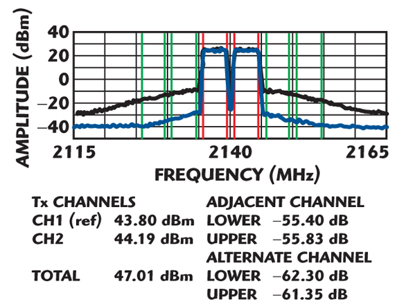
The TGH2932-FL Doherty amplifier delivered approximately 250 W of peak power and 50 W of average power with a gain of 11.5 dB. For a pre-distortion corrected ACPR of –55 and –60 dBc in the adjacent and alternate channels, respectively, this implementation delivered an unprecedented 57 percent collector efficiency.
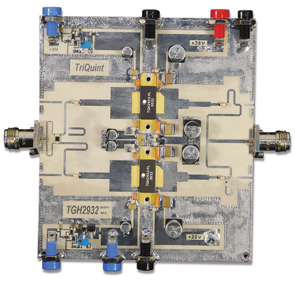
This means that to produce 50 W of RF power, the amplifier consumed only 88 W of DC power, leaving 38 W to be dissipated as heat—much less than that of a standard household light bulb. (The TGH2932-FL is shown in its Doherty evaluation board in Figure 2.)
A direct comparison of these results to published data for equivalent LDMOS or GaN devices used in a Doherty configuration is difficult to accomplish. However, a survey of the literature suggests that the HV-HBT-based Doherty holds an efficiency advantage over LDMOS of at least 10 percentage points, and over the more expensive GaN by approximately five points.1,2
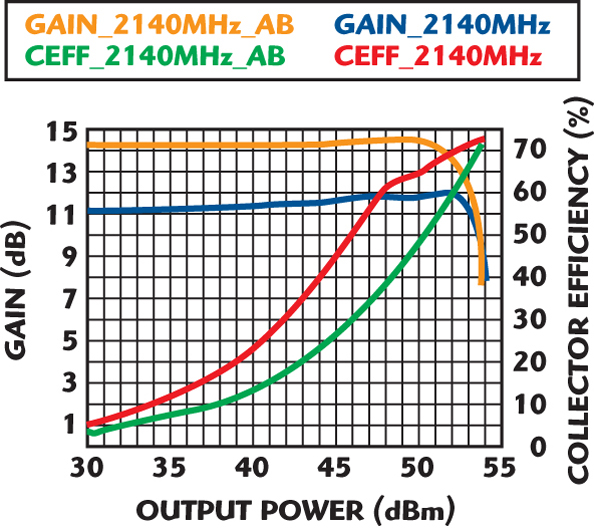
The inherent design advantages of an HV-HBT device are particularly well suited to reap the benefits of the Doherty circuit topology. As can be seen in Figure 3, the TGH2932-FL Doherty collector efficiencies are achieved over a wide range of power levels, which makes the approach highly advantageous for the very dynamic signal environments present in 3G and 4G systems.
Comparing collector efficiencies in Doherty (57%) and Class AB (34%) operation at the 47 dBm point, the HV-HBT devices dissipate 59 W less heat when used as a Doherty, more than a 60 percent savings compared to Class AB.
The truly impressive results in on-going developmental research represent the culmination of lengthy and highly focused efforts by members of a cross-functional team of process, design and application engineers. Together they modified the basic design of the HV-HBT unit cell to deliver higher efficiency, linearity and peak power.
One of the principal challenges that the team faced was an early breakdown phenomenon that was dubbed “flicker”. The breakdown would occur at voltages far below where the device needs to operate given a 28 V DC rail with a high power AC waveform riding upon it. However, the breakdown was transitory in nature, and highly unpredictable, even on a given device. By careful design and experimentation the problem of “flicker” was resolved through modification of device structures, coating layers and etch processes.
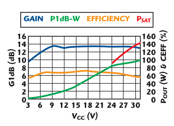
The results achieved by these demonstration HV-HBT devices indicate that they are poised to become an integral part of next-generation high efficiency power amplifier designs that utilize envelope tracking (ET) techniques to boost efficiency even further. In an ET amplifier design, RF power devices have their DC supply voltage modulated to follow the peaks and valleys of the RF signal. In other words, when the RF signal requires a high peak power, the DC supply voltage is increased to allow the peak signal to pass. When the RF signal is closer to the average power level, the DC supply voltage is lowered by a corresponding amount. By modulating the supply voltage in this fashion, circuit designers can tailor the amount of DC power available at any given instant in time to the amount of RF power that needs to be delivered, vastly improving amplifier efficiency and reducing DC power consumption. The TGH2932-FL device is very well suited for ET amplifier design applications because the gain, efficiency and linearity of the HV-HBT device remain nearly constant over a wide range of supply voltages. This allows designers more latitude in adjusting the supply voltage to match RF power demands, maximizing the resulting efficiency gains (see Figure 4).
OEM base station amplifier designers looking to unlock the potential of an ET design should consider the benefits of adopting a HV-HBT device technology. It is anticipated that efficiencies obtained using ET techniques will outstrip those achieved when utilizing a Doherty configuration.
Several design and production enhancements contributed to the success of the demonstration HV-HBT device and its ensuing product line. For example, the design employs thermal shunts to effectively remove heat from the active region of the transistor. Devices are 100 percent screened to a minimum 72 V breakdown and are compatible with existing 28 to 32 V base station power supply voltages. To ease the design burden, packages incorporate a proprietary input pre-match circuit and output-matching element. This approach allows the designer to more readily achieve excellent input and output return losses while improving manufacturability compared to conventional chip and wire solutions.
Performance was the goal when research began on a new generation of base station power amplifiers, but reliability must be assured given the inherent demands of base station manufacturing and field deployment. The intrinsically robust nature of the GaAs material, along with all-gold metallization, results in an extremely rugged device. The TGH series HBT die are treated with a surface passivation to ensure reliable operation in non-hermetic environments. Measured endurance of InGaP HBT devices exceeds 106 hours mean-time-to-failure (MTTF) at 170°C junction temperature and 10,000 hours MTTF at a 250°C junction.
The challenges in developing highly linear, reliable and efficient power amplifiers for 3G and 4G base station applications are formidable. To overcome those challenges, semiconductor device and base station design engineers will have to work together to create the next generation of devices optimized for use in more sophisticated topologies. Documented efficiencies show an advantage over competing device technologies that are available today. Results achieved by this new generation of HV-HBT InGaP GaAs power transistors are an important first step in the quest to deliver a highly efficient, reliable power amplifier that system operators are demanding. As 4G systems are deployed across the world in 2500 and 3500 MHz bands, underlying HV-HBT transistor technology can extend the realized benefits and performance into higher and higher frequencies. TriQuint is working with lead customers to define a family of HV-HBT devices covering a variety of frequency bands and power levels that will harness the capability of new and improved HV-HBT process technology, pushing the boundaries of device performance into commercially realizable designs that can be used by base station OEM amplifier manufacturers to meet challenging performance requirements head-on.
TriQuint Semiconductor Inc., Richardson, TX and Orlando, FL
(407) 886-8860,
e-mail: info-basestation@tqs.com,
www.triquint.com.
RS No. 302