
Signal source spectral quality has become the single parameter that limits achievable performance of many modern communication and radar systems. In communication systems that utilize complex modulation to achieve spectral efficiency, the achievable bit error rate (BER) is often limited by the transmitter and local oscillator phase noise. In many modern radar systems, the sub-clutter visibility, that is the ability to differentiate an object from a complex background, is similarly limited by the transmitter and local oscillator phase noise.
Reciprocal mixing is another phenomenon that causes receiver noise to increase in presence of strong signals, thereby limiting detection of weak signals in adjacent channels. The cited degradation in system performance is the result of the phase noise of the signal sources employed within the designated systems. Phase noise may also limit the maximum angular resolution, which can be achieved by an interferometer type of direction-finding receiver. Phase noise is the result of random modulation of the phase component of a signal; it is characterized by the single sideband phase noise normalized to a 1 Hz bandwidth and symbolized by  (fm). Phase noise is similar to the jitter specification common to components used within network and other high speed digital systems. Within this brief tutorial, the topic of phase noise in oscillators is explored. The indigenous sources of phase noise are disclosed and models are developed for phase noise prediction in both free-running and phase-locked oscillators from which specific low phase noise design rules are deduced. The interested reader is referred to the cited references for more detailed information.
The Scherer Equation
Phase noise is the result of random modulation of the phase component of a signal; it is characterized by the single sideband phase noise normalized to a 1 Hz bandwidth and symbolized by (fm).
The Scherer equation1 relates the phase noise of a free-running oscillator to the constituent parameters of the oscillator system, specifically the noise figure of the active element (F), the resonator quality factor (QL), the operating frequency (fo) and available power (Pav). The active element noise figure is a composite parameter that includes the ‘flicker’ or 1/f noise.
Notwithstanding the uniqueness of various oscillator circuit topologies, the circuit topology utilized for the mathematical development is based upon an explicit feedback loop containing a single-section resonator. The Scherer equation does not account for nonlinear behavior within the active element and is therefore somewhat limited with respect to highly accurate oscillator phase noise estimation in all cases. However, the utility resides within the identification of the parameters contribution and is not significantly diminished by the absence of nonlinear analysis. In addition, the Scherer equation provides an intuitive understanding of the principal factors that determine the phase noise of free-running oscillators. The development begins with an exploration of the phase modulation of a signal by additive noise and proceeds to the examination of the noise-to-signal ratio upon further processing within an explicit feedback loop containing a single-section resonator. The resonator is mathematically characterized by an equivalent low pass element to facilitate representation of phase noise by the conventional, single sideband, noise-to-carrier ratio.
The Basics
The development of the Scherer equation begins with some circuit theory basics required to establish and characterize noise, in this case the Johnson noise—also known as Nyquist or thermal noise. Noise within electrical systems is principally caused by the random thermal agitation of charges. There are other types of noise, such as shot or flicker noise, to be included in the analysis with significant impact to the overall phase noise at various offset frequencies. However, the thermal noise is the basis and accounting for flicker noise is accomplished with a modest adjustment to the active device noise figure. Figure 1 illustrates a circuit topology consisting of a series connected resistor, a bandpass filter and an RMS voltmeter.
The open circuit noise voltage of a resistor may be represented by 
where

k = Boltzmann constant (1.38E-23 Joules/K)
T = absolute temperature (K)
B = measurement bandwidth (Hz)
R = resistor value (Ω)
Referring to Figure 2, consider the maximum noise power available from the source resistor, R1. The voltage across the resistor R2 may be written as

The power dissipated in resistor R2 may be written as

The maximum available power is found by differentiating Equation 3 with respect to R2, setting the result to zero and solving for R2. Executing this procedure produces the expected result for maximum available power transmission
R2 = R1 (4)
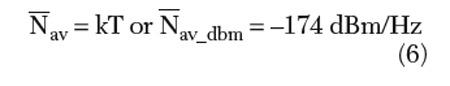
Further, upon substitution of R1 = R2 = R, the maximum available noise power may be written as
Nav = kTB (5)
This result—although obvious—facilitates further development of the phase noise of a free-running oscillator and is a fundamental element of the general topic of noise analysis. The diligent reader is referred to any of numerous available articles (for example, one might search using the text “thermal noise”). Upon normalization with respect to a 1.0 Hz bandwidth, the following result may be written
Additive Noise and Phase Modulation
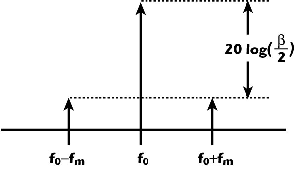
Before exploring how additive noise engenders phase modulation to a signal, a short review of elementary phase modulation theory is in order. A single tone sinusoidal signal, s(t), with phase modulation may be mathematically represented as
s(t) = αccos[2πfot + βsin(2πfmt)] (7)
If β<<1 (small modulation index), s(t) may be represented as
s(t)  αccos[(2πfot) – βsin(2πfmt)sin(2πfot)] (8)

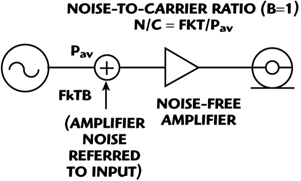
The spectral content of the signal is shown in Figure 3, where the carrier, and lower and upper sidebands are represented. Additive noise induces phase modulation sidebands on a signal. To examine and quantify this phenomenon, observe Figure 4, where a signal with available power Pav is introduced to an amplifier. The noise (normalized by a 1 Hz bandwidth) generated by the amplifier (FkT) is also referred to the input. The power spectral density of the added noise may be represented by the sum of random variable sinusoidal signals of available power, FkT, and is expressed as

Similarly,


The reason for this apparent diversion becomes evident when the phasor representation of the signal and added noise are graphically illustrated as in Figure 5. From the previously developed PM theory, the phase deviation engenders two sidebands on the carrier, displaced by the modulation frequency, fm. The total RMS phase deviation is the sum of the two sidebands, and is represented by
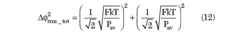

In the following descriptions, the total RMS phase deviation will not include the specific reference to ‘total’. In addition to the thermal noise with a constant power characteristic versus frequency, active devices are also characterized by a low frequency noise component, often referred to as ‘flicker’ or 1/f noise, due to the increase in noise power density as the frequency decreases. Mathematically, the 1/f noise may be accounted for by including a frequency dependent term. Accounting for the 1/f noise term, the total phase modulation may now be written as

Note that although the equation indicates an increase in noise below the cut-off frequency fc of 6 dB/octave, some devices may have a greater exponential characteristic, such as  , with 12 dB/octave or greater increase in noise density below the cut-off frequency. Bipolar junction transistors (BJT) and heterojunction bipolar transistors (HBT) are characterized by the 6 dB/octave slope and have lower cut-off frequencies than GaAs FET or PHEMT devices.

While the total phase noise-to-carrier power ratio has been mathematically represented by the double sideband symbol Δφr , phase noise is more commonly characterized using the single sideband noise-to-power ratio at a specified offset frequency, fm. The symbol (fm) represents the ratio of the single sideband power of phase noise in a 1 Hz bandwidth at fm Hz from the carrier, to the carrier power; the units are dBc/Hz. The mathematical relationship between Δφr2rms and (fm) is simply

The graphic of Figure 6 is more descriptive and offers a more intuitive definition.

Oscillator Phase Noise Model
The phase noise model for the phase feedback oscillator is illustrated in Figure 7, where an amplifier is represented with an equivalent input noise and an explicit feedback loop containing a resonator characterized by the center frequency fo, the bandwidth Bw and the loaded quality factor Ql. The output power spectrum of phase noise variation is represented by Δφ20(fm); the output power spectral density is processed by the resonator and produces an input power spectral density of phase noise variations represented by Δφ2(fm), where fm is the offset frequency from the carrier, fo. In order to work directly with the offset frequency, the bandpass characteristic of the transmission resonator is replaced by the low pass equivalent and the feedback oscillator phase noise model is modified, as shown in Figure 8. The low pass equivalent of the transmission resonator is depicted using the transfer function T(fm).

The feedback loop equation may be written as

Solving for the output power spectral density yields

The low pass transfer function may be written as

Upon substitution within the loop equation, one may write

Simplification of the equation yields

From Equation 14 developed earlier

where upon further substitution and utilization of the magnitude of the transfer function

Recall that

The Scherer equation in final form is written as

The significant parameters of the Scherer equation are summarized below:
• Select devices with low 1/f noise, such as BJT or HBT devices as opposed to GaAs FET devices
• Select large geometry devices to maximize Pav
• Maximize the resonator loaded quality factor, Q1
• Minimize the noise figure, F; this may be done by control of the impedance environment of the active device.
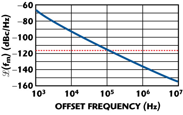
It should be remembered that the Scherer equation does not account for nonlinear conversion of noise sidebands. Notwithstanding this limitation, (fm) prediction is reasonably accurate for those applications where the feedback signal level is controlled in a manner that limits the degree of nonlinear operation. As an example, the predicted phase noise of an oscillator constructed from an InGaP HBT using a resonator with a loaded quality factor, Ql = 56, is shown in Figure 9.
Phase-locked Loop Oscillator Noise Model

The phase-locked loop circuit topology is illustrated in Figure 10, where a voltage-controlled oscillator (VCO), frequency divider, phase detector and loop amplifier are exhibited in a classic feedback loop configuration. A crystal oscillator provides a stable reference source from which an error signal is derived. The error signal is generated by the phase detector, which compares the phase difference of the VCO—appropriately divided—and the reference source. The loop amplifier conditions the error signal and corrects the phase of the VCO in accordance with the error signal. The net result of the loop action is to impart the spectral characteristics of the reference source to the VCO consistent with the bandwidth of the loop. The block diagram of the phase-locked loop noise model is shown in Figure 11, where each of the constituent component noise sources are identified in accordance with the following symbols and text:
Δφout = Output RMS phase noise
Δφosc = VCO phase noise (Δφosc = enosc Ko/s)
Δφref = Reference phase noise
Δφdiv = Frequency divider phase noise
Δφdet = Detector phase noise (Δφdet = /Kφ)
Ko = VCO gain constant (Rad/V)
Kφ = Phase detector gain constant (V/Rad)
A(s) = Loop amplifier transfer function
Eni = Amplifier equivalent input noise

The loop equation may be written by noting the phase noise at each point around the loop
At A:

At B:

At C:

At D:
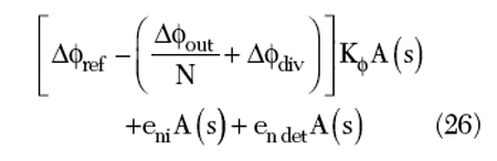
At E:
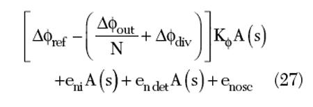
At F:

Solving for Δφout:

Making the following substitutions:

And rewriting, one obtains:
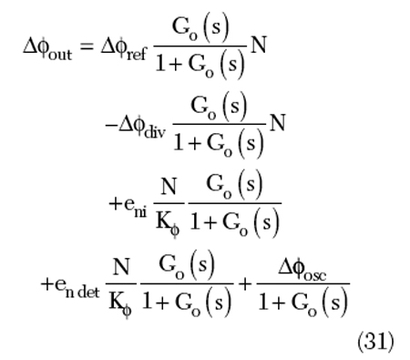
At this point, one must recognize that all the identified noise sources are uncorrelated, and therefore, may be added on an RMS basis. The output signal power spectral density may now be written as

It should be noted that the closed loop gain is a complex transfer function and the magnitude of the complex transfer function has been used.
The constituent noise contributors may now be identified, as listed in Table 1.
Upon review of the individual noise sources, the following guidelines for the design of low phase noise signal sources may be deduced:

• Minimize reference noise: Δφref
• Minimize divider modulus: N
• Maximize open loop gain: Go(s)
• Maximize phase detector gain: Kφ
• Minimize phase detector noise: endet
• Minimize amplifier input noise: eni
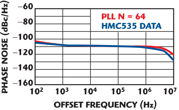
An example of a phase noise prediction using the model developed is offered. Because the phase noise parametric data and measurements are readily available on the data sheet, the phase noise estimate utilizes the Hittite Microwave HMC535 Ku-band phase-locked IC-PLL (frequency divider noise from HMC439 (InGaP)). The HMC535 is a GaAs InGaP heterojunction bipolar transistor (HBT) MMIC PLO. The power output is +9 dBm, typical from a +5 V supply voltage. All functions (VCO, op-amp, PFD and prescaler) are fully integrated with the exception of the off-chip customer specific loop components.
Additional features of the HMC535 are summarized:

• InGaP HBT technology for low 1/f noise
• Low noise Ku-band VCO
• 1/64 prescaler
• Low noise phase detector
• Low noise loop amplifier
A block diagram of the HMC535 IC-PLL configured with external loop components is shown in Figure 12. The following parameters are specified within the HMC535 data sheet:
Ko = 2π125•106 rad/V
Kφ = 1/π V/rad
N = 64
det = –150 dBc/Hz
div = –155 dBc/Hz (at 1 kHz)
eni = 2.0 nV/
ref = typical VHF crystal oscillator

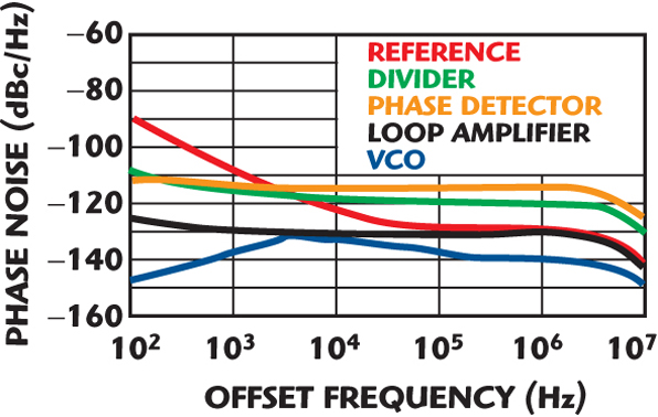
The results of the phase noise prediction are graphically illustrated in Figure 13. Note the excellent correlation at offset frequencies greater than 1 kHz. The constituent noise source contributions are graphically depicted in Figure 14. As may readily be discerned from the graphic, the principal contribution to the aggregate phase noise at offset frequencies greater than 1 kHz is the divider and phase detector noise; below 1 kHz, multiplied reference noise is the main noise contributor.
The phase noise data supplied by Hittite for the HMC535 is more typical of what one would expect of a residual phase noise measurement; that is a measurement of two sources within a source canceling phase bridge. Figure 15 shows the results from a numeric prediction using residual phase noise measurement technique. The residual phase noise estimate is executed with the reference source noise equal to zero, as that is what occurs in a good quality phase bridge. The estimate of phase noise for this example employed a loop amplifier with the controlling elements adjusted to provide a bandwidth equal to that of the Hittite application note.
The strong agreement between prediction and measurement suggests that the oscillator and other loop elements are merely mildly nonlinear.
Phase Noise Measurement
Phase noise measurements require significant care due to the low measurement levels and possible interference from the electromagnetic environment. In addition, low power supply noise and high isolation within the oscillator and external to the oscillator and measurement equipment are mandatory. There are basically two types of phase noise measurements: absolute and residual. Absolute phase noise measurement is applicable to signal sources while residual phase noise measurement applies to both signal sources and components. In addition, residual phase noise measurement generally implies the removal of the reference source via a well-balanced phase bridge utilized in the measurement.
Absolute Phase Noise Measurement
There are two common techniques employed to execute absolute phase noise measurements: The frequency discriminator method and the phase detector method.
(fm) Measurement Using a Frequency Discriminator
The frequency discriminator method uses the relationship between FM and PM within angle modulation theory. Basically, the relationship between the FM and PM indices may be mathematically described by the equation:

Therefore, the spectral density of frequency variations may be written

Recall that

Now, one may write


The output of a frequency discriminator may be written as

Kf is the discriminator gain constant. Now one may write


The test equipment block diagram is shown in Figure 16. Calibration of the frequency discriminator may be accomplished via a source excitation using a frequency synthesizer or other generator capable of precision frequency deviation. An alternate calibration technique requires low level modulation in conjunction with observation of the sideband level; this technique results from the equation
In addition to the resonator implementation of the frequency discriminator, a delay line may also be employed. The delay should be constant versus frequency and must also comply with other restrictions, the principal restriction being

where τd is the time delay
The governing equation for the delay line frequency discriminator measurement is

As one might expect, this descriptive equation is the same as the prior equation if one recognizes that the discriminator coefficient for the delay line implementation may be written as


The test equipment block diagram for the phase noise measurement using a delay line frequency discriminator is illustrated in Figure 17. The measurement of (fm) using the frequency discriminator technique is limited close to carrier due to the 1/(fm)2.
(fm) Measurement Using Phase Detector
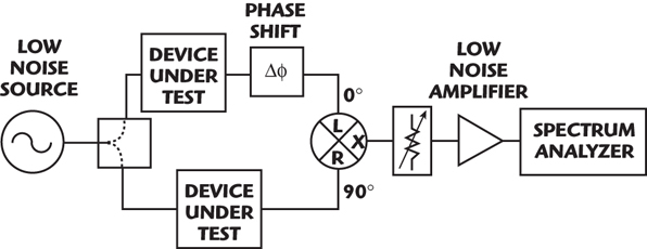
The most direct and sensitive method of phase noise measurement utilizes two sources in phase quadrature and a wide dynamic range mixer, as shown in Figure 18. The signals at the RF and LO ports of the mixer should be in phase quadrature to assure maximum sensitivity and AM rejection. If the mixer is operated linearly, the phase detection coefficient is equal to the peak sinusoidal voltage of the mixer output when the two sources are frequency offset. Because the phase noise of each source is measured in this configuration, the phase noise of one of the sources must be known to determine the phase noise of the other source. The governing equation for the phase noise measurement is

Residual Phase Noise Measurement

Residual phase noise measurements are employed to determine the degradation in spectral quality of components that are typically used in the generation of low phase noise signals; such components include amplifiers, mixers, frequency dividers and multipliers, and phase detectors. Unlike the absolute measurement of phase noise, residual phase noise measurement typically employs a phase bridge technique and cancellation of the excitation source noise. The block diagram of Figure 19 represents the test equipment configuration utilized for residual phase noise measurement. In the process of executing phase noise measurements, it is prudent to observe the following guidelines:
• When using the phase-lock technique, the offset frequency of the measurement must be much larger than the loop bandwidth.
• Insure that no injection lock phenomenon exists between the two sources.
• Minimize AM detection and maximum detection coefficient by maintenance of quadrature to within ±2°.
• Operation of the mixer in a linear mode is essential to prevent calibration and measurement errors.
• Insure that the calibration of the beat-note signal is sinusoidal.
• Insure that the entire measurement system cascade is operated in the linear range, that is with no compression.
• Impedance interfaces and power levels should remain constant during calibration and measurement.
• Insure that the source cancellation is sufficient when making residual phase noise measurements.
• Use low noise DC power supplies.
• Exercise caution with respect to co-located instrumentation, such as oscilloscopes, computer monitors, DVM and counters.
• Avoid microphonically or acoustically induced noise.
• Utilize a screen room with filtered input power and indirect lighting, when possible.
References
1. D. Scherer, “Design Principles and Test Methods for Low Noise RF and Microwave Sources,” Hewlett-Packard RF and Microwave Measurement Symposium, October 1978.*
2. J.B. Johnson, Physical Review, 32, 97, 1928, or H. Nyquist, Physical Review, 32, 110, 1928.
3. D. Scherer, “Generation of Low Phase Noise Microwave Signals,” Hewlett-Packard RF and Microwave Measurement Symposium, September 1981.*
4. W.P. Robbins, Phase Noise in Signal Sources, Peter Peregrine Ltd., London, UK, 1982.
5. D. Leeson, “A Simple Model of Feedback Oscillator Noise Spectrum,” Proceedings of the IEEE, Vol. 54, February 1966, pp. 329–330.
6. G. Sauvage, “Phase Noise in Oscillators: A Mathematical Analysis of Leeson’s Model,” IEEE Transactions on Instrumentation and Measurement, Vol. 26, No. 4, December 1977.
7. K. Kurokawa, “Some Basic Characteristics of Broadband Negative Resistance Oscillator Circuits,” Bell System Technical Journal, July-August 1969, pp. 1937–1955.
8. K. Kurokawa, “Microwave Solid State Oscillator Circuits,” Microwave Devices, Chapter 5, Howe and Morgan, Eds., John Wiley & Sons Inc., Hoboken, NJ, 1976.
9. S. Hamilton, “Microwave Oscillator Circuits,” Microwave Journal, Vol. 21, No 4, April 1978, pp. 63–66 and 84.
10. S. Hamilton, “FM and AM Noise in Microwave Oscillators,” Microwave Journal, Vol. 21, No. 6, June 1978, pp. 105–109.
11. D. Bannerjee, “PLL Performance, Simulation and Design” Fourth Edition, (c)2005.
12. K. Puglia, “Phase-locked Loop Noise Models,” Microwave Engineering Europe, December/January 1995.*
13. U. Rohde, “A New and Efficient Method of Designing Low Noise Microwave Oscillators,” PhD dissertation, Technische Universität Berlin, 2004.
14. F.M. Gardner, Phaselock Techniques, John Wiley & Sons Inc., New York, NY, 1979.
15. C. Grebenkemper, “Local Oscillator Phase Noise,” Watkins-Johnson Technical Note, Vol. 8, No. 6, November/December 1981.
*Primary sources of material for this tutorial.
 Kenneth V. Puglia holds the title of Distinguished Fellow of Technology at the M/A-COM business of Tyco Electronics. He received his BSEE (1965) and MSEE (1971) degrees from the University of Massachusetts and Northeastern University, respectively. He has worked in the field of microwave and millimeter-wave technology for 35 years and has authored or co-authored over 30 technical papers in the field of microwave and millimeter-wave subsystems. Since joining M/A-COM in 1971, he has designed several microwave components and subsystems for a variety of signal generation and processing applications in the fields of radar and communications systems. As part of a European assignment, he developed a high resolution radar sensor for a number of industrial and commercial applications. This sensor features the ability to determine object range, bearing and normal velocity in a multi-object, multi-sensor environment using very low transmit power.