
A planar composite lowpass filter implemented in microstrip line, designed by image parameter method will be described. This composite filter combines four filter sections and presents an attenuation pole near the cut off frequency to ensure sharp cut off. This filter design also ensuring good matching properties in the passband. The lumped-element schematic of the filter has been implemented, and the lumped elements are converted into microstrip line to become a planar composite filter. The simulations are done by Advanced Design System (ADS). The microstrip line simulation results shows 1.5GHz as the cut off frequency of the filter, which fulfill the design specification.
Measured results exhibit some losses compared to the simulation results, with +/- 0.1GHz tolerance from the cut off frequency and the insertion losses for the designs are around -1dB to -2 dB, which may caused by practical limitations. Measurement results exhibit rejection of the attenuated pole around 20 to 30dB.
The composite low pass filter in microstrip line with T and π network is a success with sharper cut off and less ripples in the passband. These filters have been fabricated on a FR4 substrate and perform a very low cost solution for RF applications.
I. INTRODUCTION
The electromagnetic spectrum is limited and has to be shared. Filters are used to select or confine the RF/microwave signals within assigned spectral limits. Emerging applications such as wireless communications continue to challenge RF/microwave filters with ever more stringent requirements—higher performance, smaller size, lighter weight, and lower cost [1].
Depending on the requirements and specifications, RF/microwave filters may be designed as lumped element or distributed element circuits.
They may be realized in various transmission line structures, such as waveguide, coaxial line, and microstrip line [2].
Planar microstrip filter designs are very challenging. Most conventional approaches are Butterworth or Chebyshev types, but they require a high-order design to ensure a good selectivity near the passband since they have no attenuation poles.
Elliptic-function filters have attenuation poles near their passbands, making them very attractive for high-selectivity applications.
However, a high-order design is also required to simultaneously ensure a flat response in the passband and a good out-of-band attenuation. In all cases, a compact planar design is practically hard to achieve due to the number and size of components to be implemented using the semilumped component approach.
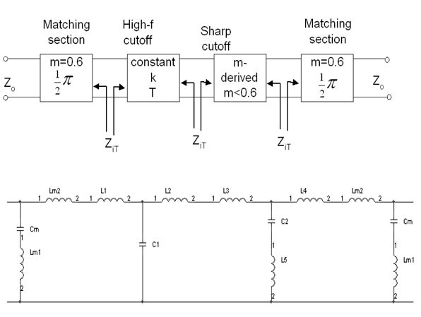
By combining in cascade the constant-k, m-derived sharp cut-off, and the m-derived matching section, a filter with desired attenuation and matching properties can be realized. This type of filter is so called the composite filter. A low pass composite filter with 1.5GHz cut off frequency and the infinite attenuation pole occurs at 1.8GHz is discussed.
While microstrip filters may take many forms, filter designs may be obtained by taking classical lumped filter design and converting them to microstrip line form, using the equivalence of short lengths of transmission line to inductance or capacitance.
The design of composite filter is using the image parameter method. This method involves the specifications of pass band and stop band characteristics of a cascade of two port network. Although this method is simple, the design of filters by this method must be iterated many times to achieve the desired results.
II. COMPOSITE LOW PASS FILTER DESIGN
There are two methods available to synthesize passive filters. One of them is known as the image parameter method and the other as the insertion-loss method.
The former provides a design that can pass or stop a certain frequency band, but its frequency response cannot be shaped. On top of that, the image parameter method of filter design involves the specification of pass band and stop band characteristics for a cascade of two-port network.[3].
The insertion-loss method provides a specified response of the filter. Nevertheless, the image parameter method is useful for simple filters and provides a link between infinite periodic structure and practical filter design[3].
Constant-k filters sections can be used to design any low pass filter and high pass filter. However, there are two major drawbacks to this type of filters: the signal attenuation rate after the cut off point is not very sharp; the image impedance is not constant with frequency.
From a design point of view, it is important that it stays constant, at least in its pass band [4]. Since constant-k filter section suffers from the disadvantages of a relatively slow attenuation rate past cut off and a non constant image impedance, m-derived filter section is a modification of the constant-k section designed to overcome these problems [3]. Therefore, 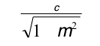
is the condition can be used to sharpen the attenuation at cut off [4]. Physically this pole in the attenuation characteristic is caused by the resonance of the series LC resonator in the shunt arm of T. This is easily verified by showing that the resonant frequency of this LC resonator is ω∞.
The position of pole at ω∞ can be controlled with the value of m. Since image impedance stays the same in two cases, this cascading will not create a new impedance-matching problem. However, we still need to address the problem of image impedance variation with frequency at the input and output ports of the network.
The image impedance of the π section with m = 0.6 remains almost constant over 90% of the pass band. [4]. The bisected π section will be used to match the constant-k of T section to the input while the other side will be used to match the m-derived of T section to the output.
Figure 1. shows the combination of four sections to become a complete low pass composite filter.
The design starts with the calculation of the constant-k section and the m-derived section in T form with respect to the desired characteristic impedance , cutoff frequency (of the constant-T section) and the parameter .
The parameter sets the placement of an attenuation pole near the cutoff frequency for a sharp attenuation response. A filter of lower order is then required for a fast attenuation rate past the cutoff frequency and the attenuation pole can be easily tuned to suppress an arbitrary unwanted frequency.
This leads to a reduction in the number of components and, therefore, a reduction of the area and the cost of the filter[9].
In the first stage of the design process, which involve the lumped component, the parameter that are set as the specifications are the cut off frequency (ƒc), infinite pole frequency (ƒ∞) and the m value for the matching sections.
The design is required to get a 1.5GHz cut off frequency of the low pass composite filter. Hence, the ωc in the formula to calculate the L and C values are substituted by 2 ƒc . The image impedance Zo has been fix to 50 ohm in all cases.
The ƒ∞ should be chosen so that ω∞ in the m-derived section will result in a value of m that is smaller than 0.6. Value of m at the matching sections for input and output should be 0.6 since this value of m provide the most constant condition over the pass band. [5].
A bisected π section used to match ZiT to Ziπ. The bisected π section will be used to match the constant-k of T section to the input while the other side will be used to match the m-derived of T section to the output.
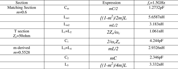
TABLE I shows the mathematical expression and value of the lumped elements.
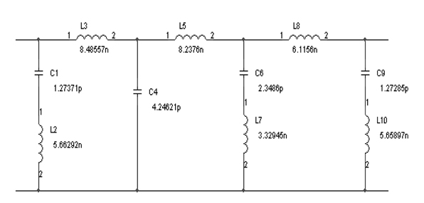
Since the inductances are in series, they can be added to a larger value of inductances. Hence, the modified composite low pass filter with T and π network is shown as the Figure 2. The values of lumped elements in Figure 2. are the values of simulation after doing some optimization using ADS.

III. IMPLEMENTATION IN MICROSTRIP LINE
In the second stage of the design process, the classical lumped filter design will be converted into microstrip line form, using the equivalence of short lengths of transmission line to inductance or capacitance[6].
To meet the requirements of high ZoL and low ZoC, assume that ZoL=100Ω and ZoC=20Ω.
As stated earlier in the design specifications, FR4 will be used and hence the εr will be 4.5, tan δ=0, a substrate thickness of 1.5mm and a conductor thickness of 35μm. By referring back to Figure 2.,
TABLE II shows the calculations for the length of the microstrip line. However, there are slightly changes in the values of the capacitors and inductors.
The values used in Table II calculations are the values obtained after the optimization in lumped circuit. The value of λd used in the calculations of the equivalence length is c/ƒ√εr=94.28mm.
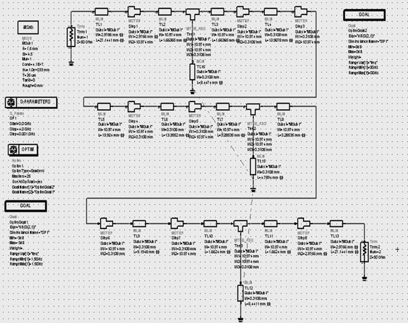
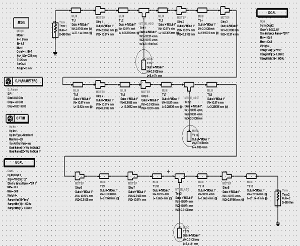
Table III shows the calculations of width for Zo, ZoL and ZoC respectively, where Zo=50ohm, ZoL=100ohm and ZoC=20ohm. Figure 3. shows the schematic of microstrip line in Design 1, while Figure 4.
shows the schematic of microstrip line in Design 2. The difference between Design 1 and Design 2 is the grounding of the microstrip line that represent the series-resonant combination in the shunt arm. In Design 1, the inductor representative microstrip line is placed with a ground in the other end while in Design 2 the ground are represented with a longer microstrip line.
IV. LAYOUT AND MOMENTUM SIMULATION RESULT FOR DESIGN 1
By using the schematic shown above, the layout can be generated using the ADS. However, the ground components should be changed to the form as shown in Figure 5.
If this is not done, the ground for lumped components will affect the momentum simulation results if apply in layout. Through holes techniques should be done on the circles in green because those holes will represent the ground.

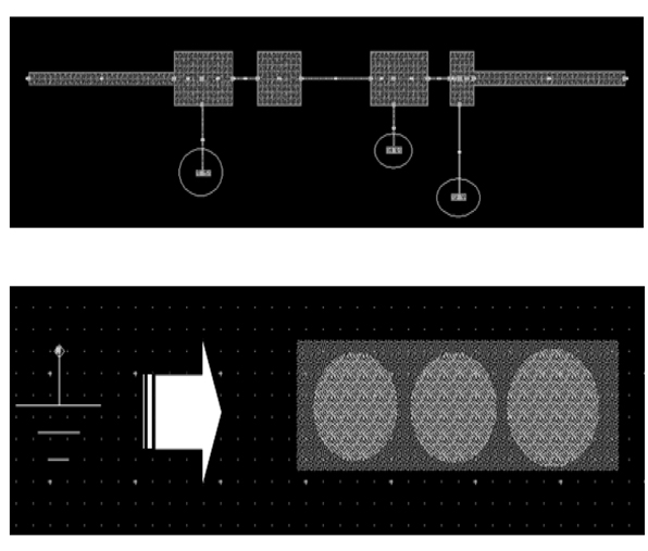
From the momentum simulation shown in Figure 6., the highest point in the pass band of the filter happened at 1.35GHz with S(2,1)= -1.46dB. To find the cut off frequency, minus 3dB from -1.46dB, which means the S(2,1) will be -4.46dB. From the graph, the cut off frequency of Design 1 occurred at 1.48GHz with S(2,1)= -4.79dB.
The difference between the microstrip S simulation result and the momentum simulation result is acceptable because the layout might not perform the dimensions until four decimal points.
V. LAYOUT AND MOMENTUM SIMULATION RESULT FOR DESIGN 2
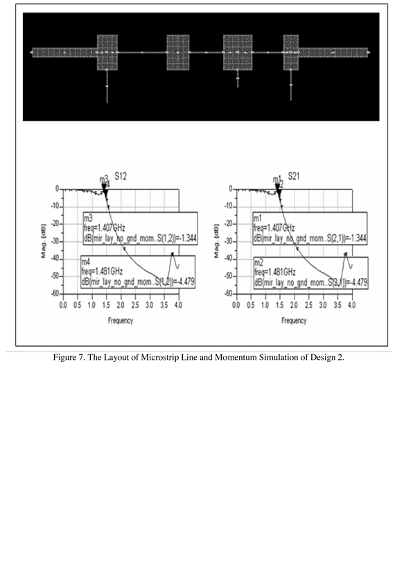
Figure 7. shows the layout of Design 2 which can be generated using ADS and the momentum simulation results of S(2,1). The pass band in Design 1 after optimization is very stable, however the frequency response does not effective for lower frequency and the circuit acts like a bandpass filter.
The reason of this situation is because of the grounding for the series resonant inductor.
This can be proved through the replacement of grounding in Design 1 with MLOC which has higher length value in Design 2. In microstrip, longer microstrip line can act as a ground and it performs better performance than grounding done in Design 1. From the simulation graph shown above, the cut off frequency happens at 1.481GHz with S(2,1)={-4.479dB-(-1.344dB)}=-3.135dB≈-3.14dB.
This simulation result is considered good even though there is a small ripple at the pass band.
VI. FABRICATION AND MEASUREMENTS
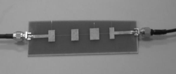
Figure 8. shows the fabricated PCB of Design 1 while Figure 9. shows the fabricated PCB of Design 2. Both designs are fabricated on FR4 and the measurement results are taken by using the network analyzer.

Figure 10. shows the measurement result from network analyzer for Design 1.
Generally, the shape of the measurement result is almost the same as the momentum simulation result. The ripples in the pass band is very small and can be assumed as negligible. Marker 1 shows the value of S(2,1) at the pass band, which is -2.48dB. For ideal case, the pass band should be at 0dB.
These may be due to the dielectric loss of the substrate. Marker 2 shows the 1.5GHz at -3.72dB, however due to the losses stated before, this point does not means the cut off frequency of the filter. The cut off frequency should hold a magnitude of -5.48dB, which is minus 3dB from marker 1.
Marker 3 shows the S(2,1) value at -5.57dB and this point shows the cut off frequency of the microstrip filter, which is 1.58GHz. Practically, this result is considered quite good for this design.
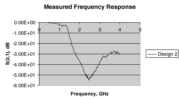
Figure 11. performs the measurement result for PCB Design 2 from the network analyzer. Comparing to the PCB of Design 1, the pass band of the signal is not that stable and it contains a small ripples. However, these ripples are still acceptable.
Marker 1 shows the frequency of 300MHz and Marker 2 shows 1.31GHz with the S(2,1) magnitude of -0.67dB and -3.28dB, respectively. Apparently, marker 3 is the cut off frequency of the microstrip filter of PCB Design 2. By minus 3dB from the S(2,1) magnitude of marker 2, we get around -6.84dB, which shown by marker 3. Therefore, the cut off frequency of this PCB is 1.40GHz.
Marker 4 shows the frequency of 1.5GHz, but the magnitude of S(2,1) is -14dB.
VII. CONCLUSION
By researching and trying on different design to convert the lumped circuit to microstrip line, the first time planar composite filter has been presented in this paper.
This composite filter has been presented using microstrip line, fabricated on FR4. The layouts have been optimized using ADS and have been validated with measurements.
The desired cut off frequency with some tolerance has been achieved. The cut off frequency in PCB Design 1 is 1.582GHz due to some unavoidable losses. On the other hand, the cut off frequency in PCB Design 2 is 1.403GHz.
In conclusion, the lowpass composite filter design work is done with success and this paper has demonstrated the potentialof using microstrip line as a low cost solution for RF planar low pass composite filter design with T and π network.
REFERENCES
[1] K. Lim, S. Pinel, M. Davis, A. Sutono, C.-H. Lee, D. Heo, A. Obatoynbo, J. Laskar,M. Tantzeris, and R. Tummala, "RF-SOP for wireless communications," IEEE Micro, vol. 3, no. 1, pp. 88–99, Mar. 2002.
[2] J.-S. Hong, M. J. Lancaster, R. B. Greed, D. Voyce, D. Jedamzik, J. A. Holland, H. J. Chaloupka, and J.-C. Mage, "Thin film HTS passive microwave components for advanced communications systems," IEEE Trans., Applied Superconductivity, 9, June 1999, 3839–3896.
[3] J.-S. Hong, M. J. Lancaster, D. Jedamzik, and R. B. Greed, "On the development of superconducting microstrip filters for mobile communications application," IEEE Trans. MTT-47, 9, 1999, 1656–1663.
[4] G. Matthaei, L. Young, and E. M. T. Jones, Microwave Filters, Impedances- Matching Networks, and Coupling Structures. Norwood, MA: Artech House, 1980, ch. 7, pp. 355–419.
[5] S. N. Uysal, "A compact coplanar stripline lowpass filter," in Asia–Pacific Microwave Conf. Dig., vol. 2, Nov.–Dec. 30–2, 1999, pp. 307–310.
[6] R. N. Martins and H. Abdalla, "Design of low-pass microstrip filters with equal-ripple passband and finite attenuation poles," in IEEE MTT-S Int. Microwave Optoelectronics Conf. Dig., vol. 1, Aug. 6–10, 2001, pp. 71–74.