
Microwave power transistors today can achieve output power levels greater than 100 W and there is more to come. In most cases, these transistors are also high voltage devices based on Si-LDMOS or GaN.
In order to characterize such transistors during development, on-wafer measurements (of sub-cells) are an indispensable tool. In this case, however, one faces the problem of how to feed the DC power safely. Typical DC voltages exceed 50 V and currents up to 10 A must be handled. Big power supplies are required, with a high amount of stored energy.
Thus, when going to the limits of the transistor, quite often the current limits adjusted by the bias compliance settings do not work properly. As a consequence, the transistors are destroyed during critical measurements. This is true also for parts of the equipment, such as the probe tips. The motivation for the development presented here is to minimize the damage in such situations, thus protecting wafer probes, bias tees, connectors and, as far as possible, the transistors themselves.
A typical RF on-wafer measurement setup is shown in Figure 1.
The device-under-test (DUT) is located on the wafer and contacted by suitable probe tips. In the following, the device is assumed to be of the HEMT type. During the measurements, the current or voltage may exceed their maximum tolerated values and a failure in the transistor or at its periphery may occur due to RF and thermal stresses. This will usually result in an excessive DC current into the drain which heats up the device, burning the drain or even causing an explosion in worst cases. Then, in general, not only is the device damaged, but so too the equipment attached, that is the on-wafer probe tips. The proposed drain current e-fuse can avoid these types of accidents in many cases. This inexpensive solution may save a great deal of time and money and avoid the loss of invaluable measurement data. The DUTs and probe tips are then safe from the transient DC peaks of the power supplies usually generated due to the high energy emission of output capacitors of the power supply. Moreover, in cases of device failure, the fast switch-off process of the e-fuse restricts the damage to its origin. Hence, the defective part can be located, which helps in detecting the sources of failure and is very important for device development.
How E-fusing Works
As discussed above, the main reason for damage is a high drain current. Thus, if the drain bias is switched off very fast, the damage can be avoided in many cases. For this purpose, two things are needed, the first of which is to follow the instantaneous drain current continuously, and the second is to switch it off very fast and efficiently, that is without any parasitic DC pulse or overshooting.
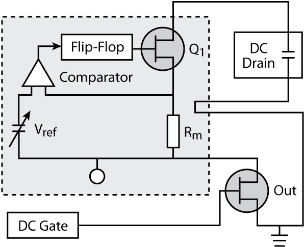
Figure 2 shows a schematic diagram of the circuit realizing these functions. The e-fuse circuit (shown in the shaded area) works as follows: The voltage across the resistor Rm is proportional to the drain current.
This voltage is monitored and compared with a variable reference voltage Vref.
If the voltage drop across Rm is higher than Vref, the flip-flop will be turned off. The transistor Q1 driven by the flip-flop will cut the drain supply of the DUT very fast.
The flip-flop can be turned on or off via the front panel. After a break action, the flip-flop must be reset or switched on for further measurements.
The essential feature of the e-fuse is its switching characteristic that should be fast and free from parasitic pulses and peaks.
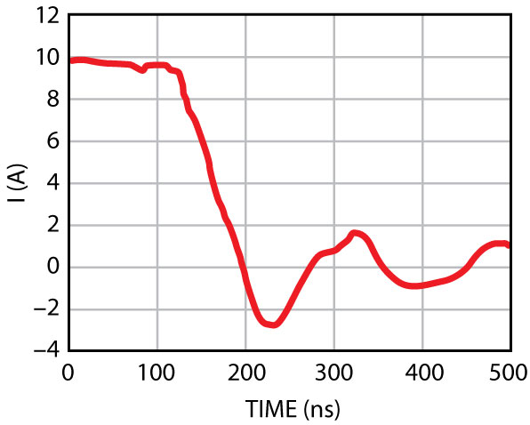
Figure 3 shows data taken from an oscilloscope. The current is shown as a function of time. Switching off 10 A of continuous current takes approximately 150 ns. One can observe that the switching is very clean in terms of unwanted pulses or peaks.
Measurement Examples
In this section, some measurements performed with and without the e-fuse connected at the drain are presented. The output capacitance of common laboratory power supplies, which is shown as Csource in Figure 4, is in the range of 1 to 10 mF.
If the drain voltage is assumed to be 28 V, the stored energy in the power supplies reaches 0.4 to 4 W. If an e-fuse is connected, Csource is isolated from the DUT.
Therefore, only the stored energy in the bias tee, that is the energy in Cbias and an additional contribution due to the switching action are effective and can damage the DUT.
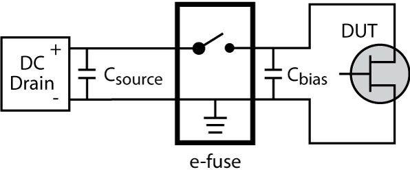
A typical bias tee has a capacitance of 10 to 100 nF, hence the energy stored is approximately 40 to 400 μW. Assuming a total short resistance of 1 Ω and a total switching time of 1 μs, there is an additional switch-off energy of about 400 μW.
Therefore, depending on the actual conditions of the devices used, applying an e-fuse drastically reduces the stored energy in the example above by a factor of 500 to 10,000.
Figure 5 shows photographs of a GaN HEMT measured without e-fuse before and after a catastrophic failure, which led to excessive drain current causing an explosion of the transistor.
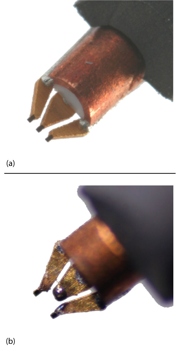
As can be seen the drain side is completely burnt out. Even worse, however, this damaged the probe tips as well. Figure 6 shows the probe before and after the failure.
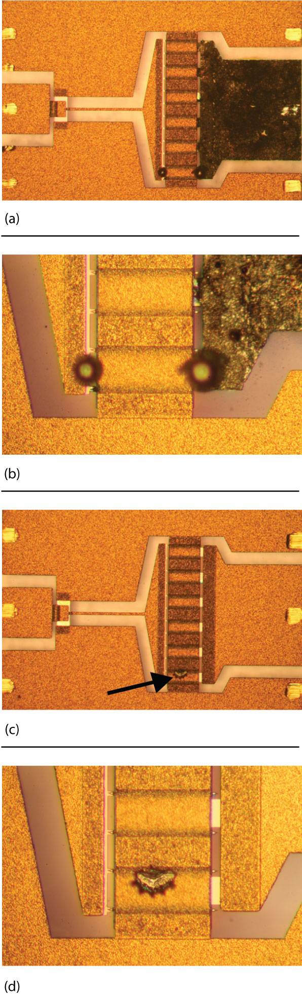
The center finger of the probe tip has simply melted and partially evaporated. This can be avoided by using the e-fuse. In the following, an example will be shown. Figure 7 illustrates the situation. Figures (a) and (b) refer to the case without e-fuse.
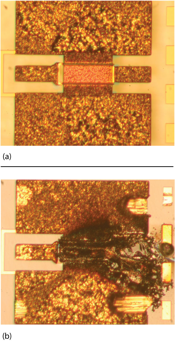
It can be seen that the drain side of the multi-finger device is burnt completely and the damage extends to the probes causing tip damage.
In contrast, Figures (c) and (d) show the results for a similar kind of problem while using the e-fuse. Only a minimum burnout has taken place, where only a single finger is damaged and the drain contact remains intact leaving the tip unaffected.
This is important not only in order to save the cost of the measurement equipment, but also because it allows better localization of the origin of the failure within the transistor. Overall, the benefits of the quick drain fusing are obvious.
Conclusion
In this article, a very effective method is presented to perform safe RF power measurements with e-fusing. Using the proposed e-fuse, it is possible to protect the measurement equipment and the devices from burnout due to excessive output current.
Thus, in case of damage, the device remains diagnosable, which helps to understand the mechanism of failure. E-fuse also protects devices from unwanted DC peaks generated from DC sources.
Such an e-fuse is particularly recommended when employing low cost DC-supplies.
References
- J.D. Brown, et al., “Performance of AlGaN/GaN HEFTs Fabricated on 100 mm Silicon Substrates for Wireless Basestation Applications,” 2004 IEEE MTT-S International Microwave Symposium Digest, Vol. 2, pp. 822–836.
- B.S. Doyle, D.B. Krakauer and K.R. Mistry, “Examination of Oxide Damage During High Current Stress of n-MOS Transistors,” IEEE Transactions on Electron Devices, Vol. 40, 1993, pp. 980–985.
- D. Park, et al., “A Full-process Damage Detection Method Using Small MOSFET and Protection Diode,” IEEE Electron Device Letters, Vol. 17, December 1996, pp. 563–565.
- S. Cripps, RF Power Amplifier for Wireless Communications, Artech House Inc., Norwood, MA, 1999.
- G. Gonzalez, Microwave Transistor Amplifiers Analysis and Design, Second Edition, Prentice Hall Inc., Upper Saddle River, NJ, 1997.
 M. Ibrahim Khalil received his BS degree in electrical and electronic engineering from I.T.T., Dhaka, Bangladesh, in 2000, and his MS degree in electrical communication engineering from the University of Kassel, Germany, in 2003. He is currently with the Ferdinand-Braun-Institut für Höchstfrequenztechnik, Berlin, Germany, where he is pursuing his PhD degree. He is working on the characterization of high power GaN transistors.
 Armin Liero received his Dipl.-Ing. degree in communication engineering from the Technische Universität Ilmenau, Germany, in 1979. From 1979 to 1989, he was responsible for the design and development of the microwave part of electron paramagnetic resonance spectrometers. Since 1989, he has collaborated on the development of a high speed digital oscilloscope. In 1995, he joined the Max-Born-Institut, Berlin, Germany, where he was responsible for the RF part of the synchronization of LASERS (MBI) and linear accelerators (DESY Hamburg). In 2002, he joined the Ferdinand-Braun-Institut für Höchstfrequenztechnik, Berlin. His current work is focused on microwave design techniques, packaging and measurements of high power transistors.
 Andreas von Müller received his Dipl.-Ing. degree in communication engineering from the Technische Universität Berlin, Germany, in 1987. From 1987 to 2002, he was responsible for the design and development of power supplies at SRM Technik GmbH, Berlin. In 2002, he founded AGIL-Electronik GmbH together with Thomas Hoffmann. Since February 2006, he is the owner-manager of AGIL-Electronik. The focus of his current work is on engineering of analog electronics for industrial applications, especially customized power supplies.
 Thomas Hoffmann received his Dipl.-Ing. degree in electrical engineering from the Technische Universität Dresden, Germany, in 1983. From 1983 to 1987, he was involved in the design and development of the electronic components of electron paramagnetic resonance spectrometers. Since 1988, he has worked on several projects as a freelance engineer, designing assemblies and devices for power electronics, especially switched-mode power supplies.