
 3D electromagnetic simulation is not only being used for the well established applications of antenna and microwave design, but issues associated with EMC, EMI, ESD and shielding also mean that it is playing an increasingly important role in the product development process across a wide range of applications. To extend its reach and to address these new areas of application the latest version of the MicroStripes full 3D electromagnetic solution—Version 7.5—boasts some major new additions.
As with its predecessors, Version 7.5 continues to use the robust and proven time domain-based Transmission Line Matrix (TLM) method for solving Maxwell’s equations initially developed by Peter B. Johns. This highly efficient technique also brings advantages when looking at transient EMI issues such as lightning, electrostatic discharge (ESD) and electromagnetic pulse (EMP).
RF Circuit Integration
Because 3D EM simulators play a supporting role to RF/microwave system and circuit design tools it is important that these 3D tools have the capability to be integrated seamlessly into existing RF/microwave design flows by working with the existing design tools. Typically, within the circuit design tools, models are built using a combination of circuit models, transmission line models and ‘black box’ devices. For more complex structures, 3D EM analysis is required for computing the device characteristics such as S-parameters that are to be used for the system analysis. This is especially important when the system being analyzed contains antenna elements and 3D geometry. With the release of Version 7.5, the integration between the simulation software and AWR’s Microwave Office® design suite has been realized. This allows the simulation software to be used from within the design environment for simulating the response of selected components within the RF/microwave circuit design. The interface automatically builds the simulation model, launches its analysis and then passes the results back to the design suite when the simulation is complete. The design suite then uses the computed characterization of the component in the circuit simulation of the entire system.
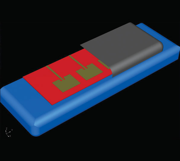
Thus, the designer has complete access to the powerful MicroStripes feature set. This allows, amongst other things, full radiation conditions to be taken into account in the antenna analysis and crucially allows full 3D geometries to be included in the model. As an example, Figure 1 shows a four-element planar patch array as imported from Microwave Office into Version 7.5, where additional 3D geometry has been added to account for the device on which the array is mounted, together with the radome.
The inclusion of the 3D geometry is critical in the antenna analysis. This is because it allows the interaction between the antenna elements and the device on which they are mounted to be accounted for in the simulation and for the fully installed characteristics to be computed.
The result of this integration moves Flomerics’ high frequency EM offering from a leading EM tool to a solution that can play a key part in a true RF/microwave integrated design environment.
EMC and Shielding
Following the introduction of the EMC directive in Europe back in the mid-1990s, many organizations are now realizing the benefit of including 3D electromagnetic analysis in the EMC design process. EMC, of course, extends beyond the test and measurement requirements of the various standards and MicroStripes 7.5 is well suited to assist with a wide range of EMC issues such as enclosure shielding, component (heat sink, for example) emissions, trace and via impedances, cable coupling and system emission analysis.
When tackling the simulation of EMC issues in 3D, it is important that the system model contains all the features that are going to influence the performance. Quite often these can be geometrically very fine and therefore need to be represented in a very efficient computational way. As such, included within Version 7.5 are a series of compact models that allow geometrically fine but electrically important features to be included in the model without the need to locally refine them.
These include the ability to model wires and wire bundles, thin film materials, slots, seams and perforated plates. By using the compact models within the simulation software it is possible to account for these items and the coupling between them and the associated structures and fields much more efficiently than if they were modeled in detail. Also, PCBs, even if well designed, will inherently be a source of electromagnetic emission in an electronics system due to the components mounted on the board, exposed traces and interconnecting cables. Within a 3D electromagnetic environment, modeling the fully detailed PCB board is a computationally intensive and extremely challenging task. Not only are there many hundreds, if not thousands, of nets on the board, there could also be several layers and many components.
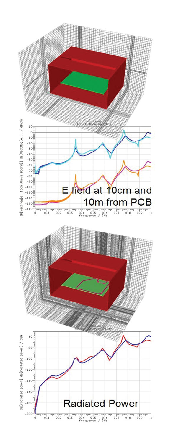
This results in some extremely fine geometric features, which make 3D analysis unsuitable for fully detailed PCB analysis.
While in a 3D solution, the sources could be approximated by means of simple wire sources, which does not account for the complex, frequency dependant, distributed nature of the PCB source.
However, Version 7.5 has the ability to import the frequency dependant, distributed EM characteristics of PCBs, to act as sources for the analysis.
Figure 2 shows how using compact sources to represent the complex frequency dependant distributed sources of PCBs results in more efficient solutions while maintaining the accuracy by replacing detailed geometric PCB models with an equivalent volume source that does not require geometric detail.
Not only does this provide a much more representative source for the system level calculation, it also allows the complex distributed source characteristics of PCBs to be included in larger system level models without having to model the details of the PCB, thereby making the simulation highly efficient.
This compact source technology can also be used directly within the simulation software, enabling designers to capture the response of an antenna and then use that response to drive an installed environment calculation. Once calculated, the compact source can be used time and time again without having to recalculate the characteristics. As such, the computational efficiency of simulations looking at antenna placement or radome effects can be dramatically improved.
As with the integration between MicroStripes and Microwave Office, this link with PCB-specific analysis tools such as PCBMod from SimLab, positions Version 7.5 firmly within the electronics EMC design flow. This allows designers to assess EMC issues much earlier in the product development process, making EMC a design issue rather than purely an end of design process test and measurement issue.
EMI
The ability to model for EMI issues is becoming increasingly important, especially for organizations involved in the military and aerospace sectors.
The requirements being placed on electronic equipment means that they now have to assess their products for issues such as EMP and lightning. Both of these are time domain-based transient effects and the TLM solver technology used within Version 7.5 lends itself very effectively and efficiently to the solution of these problems.
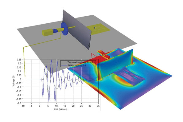
Figure 3 illustrates how the time domain-based TLM method allows transient issues such as ESD to be efficiently simulated.
Typically, within a time domain-based solution, an impulsive excitation is used which allows a wide band frequency domain analysis to be very efficiently performed.
This impulsive excitation effectively gives a constant amplitude excitation across the frequency band of interest. However, transient issues such as EMP and lightning are not impulsive in nature because they typically have a double exponential style of waveform.
Figure 4 demonstrates lightning strike analysis on a mobile phone antenna mast.
As such, with transient issues, the ability to be able to excite the model with the correct waveform is crucial as this then ensures that the calculated results will be representative.
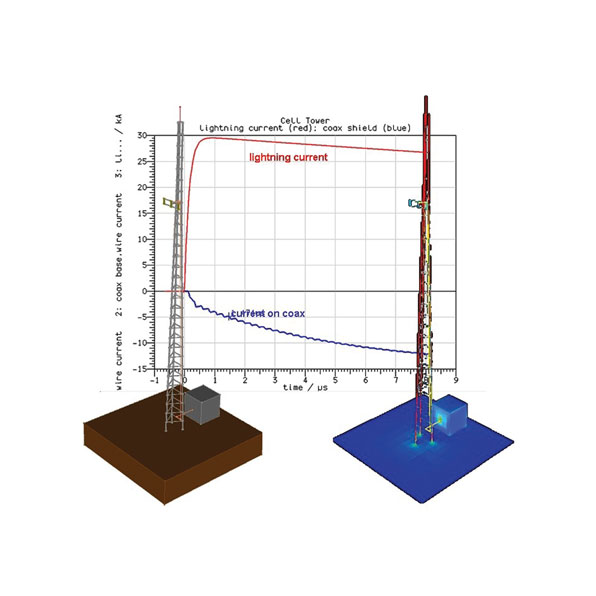
Within the MicroStripes solution, it is possible for the user to define their own time domain waveforms and attach them to the sources in the model.
By driving the simulation directly with the user specified waveforms, which can be created either from a series of predetermined waveforms or imported as a csv file, not only do the time domain results reflect that waveform but so do the field and surface current distributions at a specific moment in time, or at specific frequencies. This capability to perform transient analysis has been widely used for a range of different applications including EMP analysis of military vehicles and aircraft, lightning analysis of antenna masts and ships, as well as looking at ESD issues associated with electronic equipment.
Conclusion
The highly efficient TLM solver technology, developed over the past 30 years, remains at the core of MicroStripes 7.5 and continues to increase in efficiency, enabling users to tackle increasingly complex problems. The new and enhanced functionality within this latest version of the simulation software not only keeps the solution incredibly efficient for antenna and microwave analysis, but also allows it to be used for a greater range of EM issues such as those associated with EMC and EMI. By integrating with other leading design tools in the RF/microwave and electronics EMC design process, it is now part of a fully integrated design flow process.
Flomerics EM LOB,
Hampton Court, Surrey, UK
Tel: + 44 20 8487 3000,
Fax: +44 20 8487 3001,
e-mail: info@flomerics.com;
web site: .
RS No. 301