
Wilkinson power dividers1 have been widely used for signal division/coupling in power amplifiers (PA),2 balanced amplifiers and balanced mixers.3 The development of highly miniaturized, on-chip, power dividers is indispensable for application to silicon radio frequency integrated circuits (RFIC). With the evolution of silicon CMOS device process technology, highly integrated silicon ICs, including RF and baseband blocks, have been developed.4 However, in spite of the growth of the silicon integration technology, conventional Wilkinson power dividers, employing quarter wavelength lines, have been fabricated outside of RFIC, due to their large size, which has been an obstacle to a realization of a fully integrated silicon front-end.
In this work, to miniaturize the power divider, short wavelength coplanar waveguides, employing a periodic structure, have been used. The periodic structure was optimally designed so that the coplanar waveguide shows much shorter wavelength than a conventional transmission line. Using the optimally designed periodic structure, a highly miniaturized on-chip Wilkinson power divider was realized on silicon RFICs. To miniaturize the power divider, a coplanar waveguide, employing periodically arrayed ground structures, was optimally designed. The size of the on-chip Wilkinson power divider was 4.8 percent of a conventional one.
Structure of Coplanar Waveguides Employing PAGS
Transmission lines employing periodic structures have been fabricated on compound semiconducting substrates5,6 and silicon substrates.7,8 Transmission lines employing a periodic structure on silicon substrate have shown a low loss characteristic as well as a slow-wave characteristic.7 For this reason, the transmission lines employing periodic structures were used for this application to miniaturize on-chip passive components on a silicon substrate.8 In this work, transmission lines employing PAGS structures8 have been used for application to a miniaturized on-chip Wilkinson power divider on a silicon substrate.
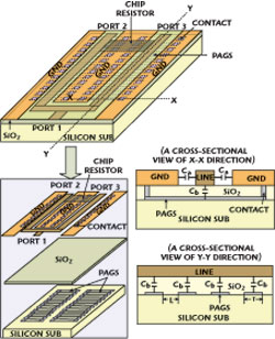
Fig. 1 On-chip Wilkinson power divider employing PAGS on a silicon substrate.
Figure 1 shows the on-chip Wilkinson power divider employing PAGS on a silicon substrate. As shown, the Wilkinson power divider consists of two section transmission lines with a length of λ/4. Each transmission line was realized using a coplanar waveguide employing PAGS. Although a conventional Wilkinson power divider occupies a very large area on a RF circuit,1 the size of the Wilkinson power divider employing PAGS was highly reduced due to a short wavelength characteristic of the coplanar waveguide employing PAGS. The reason for size reduction of the Wilkinson power divider employing PAGS can be explained as follows: As shown in Figure 1, PAGS exists at the interface between the SiO2 film and the silicon substrate, and is electrically connected to the top-side ground planes (GND planes) through the contacts (vias). Therefore, PAGS is grounded to the GND planes. As is well known, a conventional coplanar waveguide without PAGS has only a periodic capacitance Ca per unit length, while the coplanar waveguide employing PAGS has an additional capacitance Cb as well as Ca. As shown, Cb is the capacitance between the line and PAGS. In other words, the total capacitance (per unit length) of the coplanar waveguide employing PAGS corresponds to Ca + Cb, but the total capacitance of a conventional coplanar waveguide without PAGS corresponds to Ca. Therefore, the coplanar waveguide employing PAGS exhibits a wavelength (λg) much shorter than a conventional coplanar waveguide, because λg is inversely proportional to the periodic capacitance. In other words, λg = 1/[f(LC)0.5].
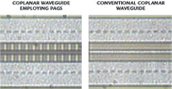
Fig. 2 Photographs of a coplanar waveguide employing PAGS and a conventional one.
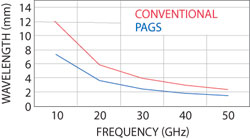
Fig. 3 Measured wavelength of the coplanar waveguide employing PAGS and a conventional one.
The wavelength of coplanar waveguide employing PAGS was compared with a conventional coplanar waveguide. Figure 2 shows photographs of a coplanar waveguide employing PAGS and a conventional one. Figure 3 shows the measured wavelength of the coplanar waveguide employing PAGS and a conventional one. The coplanar waveguides were fabricated on a silicon substrate with a height of 600 μm. L and W are 20 μm. As shown, the wavelength of the coplanar waveguide was reduced to 60 to 65 percent of the conventional one by using PAGS. For example, the wavelength of the coplanar waveguide employing PAGS (with a T of 20 mm) is 3.7 mm at 20 GHz, while the wavelength of the conventional coplanar waveguide without is 5.9 mm at the same frequency. The above results indicate that highly miniaturized passive circuits can be realized by using the coplanar waveguide employing PAGS.
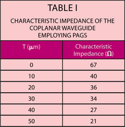
Table 1 shows the characteristic impedance of the coplanar waveguide employing PAGS. It can be seen that an increase of the strip width T results in an enhancement of the periodic capacitance Cb, owing to an increase in capacitive area. Therefore, as shown in the table, the characteristic impedance Z0 of the coplanar waveguide employing PAGS can be easily controlled by changing the strip width T, because Z0 depends on the periodic capacitance of the transmission line. These results indicate that highly miniaturized passive components with various impedances can be realized using the coplanar waveguide employing PAGS.
RF Characteristics of a Coplanar Waveguide with Various PAGS Structures
In order to select an optimal structure of the PAGS, coplanar waveguides employing various types of PAGS structures were prepared. Figure 4 shows coplanar waveguides employing various types of PAGS structures. Compared with Case 1, contacts between PAGS and ground were removed in Case 2, and slots were added in Case 3. Figures 5 and 6 show the wavelength and insertion loss of the coplanar waveguides employing the three types of PAGS structures. Case 1 shows the shortest wavelength of all types. Case 3 shows a wavelength longer than the other types.
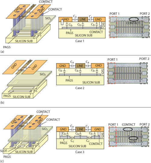
Fig. 4 Coplanar waveguides employing PAGS structures.
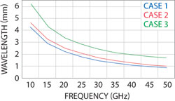
Fig. 5 Wavelength vs. frequency of the coplanar waveguides employing three types of PAGS structures.
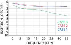
Fig. 6 Insertion loss of the coplanar waveguides employing three types of PAGS structures.
As shown, Case 3 shows an insertion loss higher than other types, because the slots on periodic ground strips cause parasitic coupling capacitances, resulting in high loss. According to these results, Case 1 shows the best performances compared with other types. It can be explained as follows. For Case 2, the PAGS was not completely grounded due to the isolation between the PAGS and the GND metal. Also, for Case 3, the middle section of PAGS was isolated from the ground due to the slots, which resulted in an incomplete ground condition. In addition, the slots on the PAGS caused parasitic coupling capacitance, which deteriorated the RF performance. For Case 1, the PAGS was connected to the ground metal through the contacts and there is no slot on the PAGS, which resulted in the best ground condition. In this work, using Case 1, a highly miniaturized Wilkinson power divider was fabricated on a silicon RFIC.
Highly Miniaturized On-chip Wilkinson Power Divider Employing PAGS

Fig. 7 Photograph of the on-chip Wilkinson power divider using PAGS.
Figure 7 shows a photograph of the on-chip Wilkinson power divider employing PAGS on a silicon RFIC. Because the port impedance was set to 27 Ω for low impedance matching applications, the characteristic impedance of transmission lines comprising the power divider are 38 Ω, and the resistor at the output ports is 54 Ω. In order to realize the coplanar waveguide with a 38 Ω impedance, the value of T was set to 20 µm, according to Table 1. In the case of a center frequency of 40 GHz, the size of the power divider employing PAGS was 0.44 × 0.1 mm2, which is 4.8 percent of the size of the one fabricated by a conventional coplanar waveguide method 1. In other words, in the case where the Wilkinson power divider is fabricated with a conventional coplanar waveguide (having a G of 30 μm) on a silicon substrate with a height of 600 μm, the length of a λ/4 line is 0.751 mm at a center frequency of 40 GHz, and the line width W is 580 μm for a characteristic impedance of 27 Ω. Therefore, the size of Wilkinson divider employing conventional coplanar waveguide is 0.916 mm2. The size comparison of the Wilkinson divider is summarized in Table 2. Figure 8 shows the power division and isolation characteristics of the Wilkinson divider employing PAGS. Good power division characteristics can be observed from 25 to 50 GHz. Specifically, S21 and S31 exhibit a magnitude of 4.5 dB at 40 GHz. In the frequency range of 25 to 50 GHz, S21 and S31 show a magnitude of 4.5 6 1 dB. The power division of the Wilkinson divider fabricated on a Teflon substrate4 is approximately −4 6 1 dB and the Wilkinson divider employing PAGS shows a loss higher by 0.5 dB than a conventional one, which originates from the high conductivity of the silicon substrate.4 The isolation (S23) shows a value of −16.2 dB at 40 GHz, and an isolation characteristic higher than −10.5 dB in the range of 20 to 50 GHz can be observed. Figure 9 shows the phase division characteristic of the Wilkinson divider employing PAGS. The phase difference between the signals at the output ports (port 2 and 3) was measured when the input signal is excited at port 1. Equal phase division characteristics, 0 ± 0.3° in the range of 20 to 50 GHz can be observed.
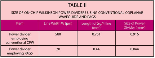
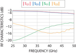
Fig. 8 Power division and isolation characteristics of the Wilkinson power divider using PAGS on a silicon RFIC.
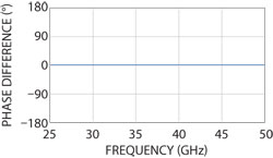
Fig. 9 Phase division characteristic of the Wilkinson power divider using PAGS.
Conclusion
In this work, a highly miniaturized on-chip Wilkinson power divider was fabricated, using a coplanar waveguide employing a PAGS on a silicon RFIC. For size reduction and low loss of the Wilkinson power divider, the RF characteristics of coplanar waveguides employing various types of PAGS structures were investigated, and an optimal structure of the PAGS was extracted. The Wilkinson power divider employing the optimal PAGS structure exhibited good RF performances from 25 to 50 GHz, and its size was 0.044 mm2, which was 4.8 percent of a conventional one.
Acknowledgment
This work was sponsored by the Korean Ministry of Education, Science and Technology Grant (The Regional Core Research Program/Institute of Logistics Information Technology). This research was supported by Basic Science Research Program through the National Research Foundation of Korea (NRF), funded by the Ministry of Education, Science and Technology (2010-0007452). This work was financially supported by the Ministry of Knowledge Economy (MKE) and the Korea Industrial Technology Foundation (KOTEF) through the Human Resource Training Project for Strategic Technology.
References
1. E.J. Wilkinson, “An N-way Hybrid Power Divider,” IRE Transactions on Microwave Theory and Techniques, Vol. 8, No. 6, June 1960, pp. 116-118.
2. D.R. Webster, G. Ataei and D.G. Haigh, “Low-distortion MMIC Power Amplifier Using a New Form of Derivative Superposition,” IEEE Transactions on Microwave Theory and Techniques, Vol. 49, No. 2, February 2001, pp. 328-332.
3. Y. Yun, T. Fukuda, T. Kunihisa and O. Ishikawa, “A High Performance Downconverter MMIC for DBS Applications,” IEICE Transactions on Electronics, Vol. E84-C, No. 11, November 2001, pp. 1679-1688.
4. M. Zargari and D. Su, “Challenges in Designing CMOS Wireless Systems-on-a-chip,” IEICE Transactions on Electronics, Vol. E90-C, 2007, pp. 1142-1148.
5. H. Hasegawa, “Cross-Tie Slow-Wave Coplanar Waveguide on Semi-insulating GaAs Substrate,” Electronics Letters, Vol. 17, No. 25, December 1981, pp. 940-941.
6. Y. Yun, J.W. Jung, K.M. Kim, H.C. Kim, W. J. Jang, H.G. Ji and H.K. Ahn, “Experimental Study on Isolation Characteristics Between Adjacent Microstrip Lines Employing Periodically Perforated Ground Metal for Application to Highly Integrated GaAs MMICs,” IEEE Microwave and Wireless Components Letters, Vol. 17, No. 10, October 2007, pp. 703-705.
7. T.S.D. Cheung and J.R. Long, “Shielded Passive Devices for Silicon-Based Monolithic Microwave and Millimeter-Wave Integrated Circuits,” IEEE Journal of Solid-State Circuits, Vol. 41, No. 5, May 2006, pp. 1183-1200.
8. Y. Yun, Y.B. Park, S.K. Kang, I.H. Kang, J.W. Jung and K.H. Park “Miniaturized On-chip Branch-line Coupler Employing Periodically Arrayed Grounded-strip Structure for Application to Silicon RFIC,” Microwave Journal, Vol. 52, No. 12, December 2009, pp. 90-98.
Jeong-Gab Ju received his bachelor’s degree in radio communication and engineering from Korea Maritime University, in 2010, and is working toward his master’s degree at Korea Maritime University.
Young Yun received his bachelor’s degree in electronic engineering from Yonsei University, Seoul, Korea, in 1993, his master’s degree in electrical and electronic engineering from Pohang University of Science and Technology, Pohang, Korea, in 1995 and his doctorate in electrical engineering from Osaka University, Osaka, Japan, in 1999. From 1999 to 2003, he worked as an engineer in Matsushita Electric Industrial Co. Ltd. (Panasonic), Osaka, Japan, where he was engaged in the research and development of monolithic microwave ICs (MMIC) for wireless communications. In 2003, he joined the Department of Radio Sciences and Engineering, Korea Maritime University, in Busan, Korea. He is currently an associate professor and his research interests include design and measurement for RF/microwave and millimeter-wave IC, and design and fabrication for HEMT and HBT.
Young-Bae Park received his bachelor’s and master’s degrees in radio sciences and engineering from Korea Maritime University in 2005 and 2007, respectively. He is currently working toward a doctorate degree at Korea Maritime University.
Suk-Youb Kang received his bachelor’s degree in electronics engineering from the University of Inchon, Inchon, Korea, in 1997, and his master’s and doctorate degrees in electronics engineering from the Inha University, Inchon, Korea, in 1999 and 2005, respectively. From 2006 to 2010, he worked as a research professor at the department of radio sciences and engineering, Korea Maritime University in Busan, Korea. Since 2001, he has held the position of representative director of INTECH Inc. and head of the Electronics and Telecommunications Research Institute. His research interests include design and fabrication for microwave/wireless communication systems and various antennas.