
Efficiency, output power and compactness are the most important parameters of a system for RF/microwave transmitter applications.
The power amplifier consumes most of the DC power in a transponder. Thus, much attention is required to maximize the efficiency of the power amplifier.
A high efficiency power amplifier allows compact and lightweight power sources, and reduces the cooling requirements. An active antenna, integrated with a power amplifier, addresses all these requirements. The choice of the antenna structure, the class of operation and heat sinking of the power amplifier, the design and simulation tools to simulate the integrated active antenna system and the testing methodology, are all major issues to develop a successful antenna integrated with a power amplifier.
The choice of planar antenna affects the design topology and system performance, due to the direct integration of the active devices and their associated matching circuits with the antenna. Another important area is the use of simulation tools to analyze an active integrated antenna (AIA) system as an entity1.
Conventionally, the antenna structure and active circuits are analyzed separately and then integrated together. This procedure results in significant deviation from predicted results when both antenna and active circuits are integrated.
Consequently, the analysis and optimization of the integrated active circuit with the antenna are required at the design level itself. Solid-state systems are more desirable in terms of size, weight, reliability and manufacturability, using mass production technology.
The main limitations of solid-state power devices are their limited power output capability along with a downward trend with frequency.2To meet the high power requirements of a system, the powers from many individual devices must be combined coherently.
Many circuit-based power-combining techniques, using different types of combiner networks, increase the overall output power. However, this technique suffers from efficiency degradation due to the loss in combiner networks. The problem becomes more serious when more and more devices are required to be combined for the same level of output power when the operating frequency is increased.

An AIA technique, with spatial power-combining technology, addresses all these limitations. In a spatial power-combining technique, the energy is combined in the low loss air dielectric medium, as shown in Figure 1. Thus, the combining efficiency will be extremely high.
The reduction of combining losses therefore enables one to achieve a high output power with overall high efficiency by combining a large number of solid-state devices, as required in high frequency operation.
A lossy feed network is retained at the input of the power amplifiers to ease phase matching. Any losses in the input feed network can be compensated by pre-amplification of the input signal, without seriously degrading the system efficiency.
An active integrated antenna array, with spatial power combining, solves the limitation of the output power handling capability of the solid-state power amplifiers, but it introduces new problems at the same time. There are many design and characterization related issues. The choice of antenna structure, the antenna feed system and the substrate materials used are vital parameters for designing an active integrated antenna system.
Different types of antenna feeds, with their merits and demerits, have been discussed in the literature.3–8 The radiation effects in a compact antenna integrated with an amplifier have been analyzed and discussed.9,10 To design an AIA system with a power amplifier, the use of a simulation tool to analyze the whole system is also very important, since harmonic balance analysis is required for the power amplifier, whereas electromagnetic analysis is required for the antenna. Characterizing the AIA with a power amplifier is not a conventional procedure since the antenna provides a dynamic load to the amplifier, instead of a fixed 50 Ω load as in the case of a conventional amplifier.
Design Related Issues
The choice of a planar antenna affects the design topology and system performance due to the direct integration of active devices and their associated biasing and matching circuits with the antenna. The class of operation of the power amplifier and the heat dissipation within the device are also major issues for designing a power amplifier integrated with an antenna.
Another important area is the use of simulation tools for analyzing the active integrated antenna system as an entity.
Antenna Structure
With the increase in operating frequency, the size of the antenna is reduced and becomes comparable to the size of the active circuits including the bias and matching networks.
Therefore, unwanted radiation from the circuits associated with the active devices will disturb the main and side lobes of the antenna. This effect can be reduced by increasing the spacing between the array elements. Another way is to use a multi-layer substrate with a low dielectric constant substrate for the antenna elements and a high dielectric constant substrate for the associated active circuits.
This will reduce the size of the active circuits compared to the antenna elements. To achieve greater bandwidth, a thicker substrate for the microstrip antenna is required. With the increase of substrate thickness, the tendency for surface-wave mode propagation increases, causing unwanted coupling among the antenna elements and with the matching circuit elements of the active circuits.
The use of a lower dielectric constant substrate reduces the coupling among the antenna elements without affecting the bandwidth of the antenna. Different architectures of active antennas with amplifiers have been discussed.11–13 Reactive-type matching networks are mainly used for input and output matching of the amplifier to achieve maximum power transfer to the antenna. Open circuit stubs are popular for matching purposes. These stubs radiate energy due to the generation of standing waves within them.
The unwanted radiation from these matching circuits not only distorts the antenna pattern but also increases the cross-polarization level. One way to minimize the unwanted radiation is to use balanced stubs for matching purposes. However, a better way to eliminate the coupling radiation between the matching network and the antenna is the use of an aperture-coupled antenna with active circuits and feeds on the opposite side of the patch.
The ground plane, between the patch and matching networks, eliminates the coupling.
Amplifier Operation and Heat Sinking
Different types of architectures for antennas integrated with amplifiers have been discussed.14–19 Efficiency is one of the main parameters of the power amplifier, which determines the DC power requirement of the transmitter. A high efficiency power amplifier not only reduces the DC power consumption, but also reduces the cooling requirements. Power amplifier operation in a switching mode is a popular technique to achieve high efficiency. Power amplifiers operating in class-D and -E provide a very high efficiency.
In both operations, the transistor is operated as a switch, in such a manner that the time domain current and voltage waveforms overlap minimally during a period. Thus, the power dissipation within the device will be ideally zero and the amplifier efficiency becomes close to 100 percent.
At microwave and higher frequencies, however, it becomes difficult to find transistors capable of switching as fast as required for class-D and -E operation. Moreover, microwave transistors have a finite ‘on’ resistance with a finite switching time, thus it is not possible to achieve 100 percent efficiency of the microwave amplifiers.
The efficiency also decreases with increasing frequency of operation. Among the different classes of power amplifiers, class-F operation has become very popular for its high efficiency and high output power capability at microwave and higher frequency operation.
In this class of operation, it is required to control the load impedances at a finite number of harmonics, which is possible for microwave devices.20,21 In class-F operation, a harmonic resonator in the output-matching network is used to shape the drain waveforms such that the load impedance provides a short at even harmonics and an open at odd harmonics.
Most power amplifiers have used transmission line networks to control the impedances at only the second and third harmonics and have achieved a higher efficiency. However, to meet the linearity requirement with moderate efficiency of communication systems, it is generally preferred to operate the power amplifiers in class AB, up to a gain compression of –2 dB. The decrease in DC-to-RF efficiency of the amplifiers with the increase in operating frequency causes the generation of more heat energy within the device. Heat sinking is one of the most critical issues for the design of a power amplifier integrated with an antenna. There are many solutions for heat sinking of the active antenna system. One way is the use of a good thermal conducting substrate, such as aluminum nitride, with a provision of more ground area for the planar microstrip antenna. The active devices, mounted/soldered on the substrate, dissipate heat through the high thermal conduction substrate to the metallic ground plane. Another solution is the mounting/brazing of flip-chip mounted or plated heat sink power devices, directly on the ground plane of the planar antenna structure, providing a heat dissipation path from the ground plane to the metallic package.
Design and Simulation Tool
In conventional amplifier design, the load impedance of the circuit is always 50 Ω(over a wide range of frequencies). However, in an AIA system, the load of the power amplifier is the input impedance of the antenna, with a limited bandwidth and a number of resonant impedances.
To ensure the out-of-band stability of the amplifier integrated with an antenna, the antenna should be modeled for its in-band as well as out-of-band response, including its multiple resonance characteristics. Linear circuit analysis is not valid to analyze power amplifiers since power amplifiers are operated in nonlinear conditions to achieve better efficiency and higher output power, instead of maximum gain as in the case of linear amplifiers. Therefore, S-parameter linear analysis cannot be used to design and simulate the power amplifiers. Conventionally, the in-band properties of an antenna are obtained from simple analysis and the effects of their out-of-band properties are ignored during the design phase of the amplifier. The design is then verified experimentally and further modifications are incorporated, based on the measurement results. The main reason for doing so is that the output port of the antenna is located in free space.
Thus, proper simulation tools are required to design and simulate the active antenna integrated with the power amplifier, to handle the nonlinearities of the amplifier and the electromagnetic properties of the antenna simultaneously. One method is to extract the broadband frequency response of the antenna as an S-parameter file, and use this file in the linear circuit simulator to analyze the complete circuit. However, this approach is not completely valid for the nonlinear operation of the power amplifier and the electromagnetic coupling among the circuit elements is also not taken into account.
Here, an improved technique is proposed to analyze the active antenna integrated with the power amplifier, using a harmonic balance analysis and an EM simulator simultaneously, for nonlinear analysis of the power amplifier and EM simulation of the planar antenna. Agilent’s design software ADS2005A has a special feature for EM co-simulation facility.
This tool allows simulation of the circuit, partly in an EM environment and partly in a circuit simulation environment. In this case, the planar antenna structure and the matching circuits (excluding lumped elements) can be analyzed by the EM simulator and the over-all response analyzed by the harmonic balance analyzer (HB) to take care of the nonlinear characteristics of the power amplifier.
Testing Related Issues
Conventionally, microwave circuits are always tested in a 50 Ω environment, and the measuring instruments are meant for that purpose. As mentioned in the previous sections, the load of the power amplifier, that is the input impedance of the antenna, has a multiple resonance characteristic. Such a complex load cannot be modeled and fabricated to replace the antenna physically while characterizing the amplifier separately. Thus, it is difficult to measure the output power delivered to the antenna directly. All the testing and measurements will be similar to the antenna measurement technique and the power amplifier parameter measurement will be an indirect measurement, based on the Friis transmission equation in antenna theory.
Design and Simulation of an Active Antenna Integrated with a Power Amplifier
The design and simulation of an active antenna integrated with a power amplifier is presented in this section. An aperture-coupled microstrip patch antenna is selected as the radiator and an MGF2430 MESFET device from Mitsubishi Electric Corp. (MELCO) is used as a power device, to demonstrate the design procedure and obtain simulation results for an active antenna integrated with a power amplifier.

Antenna Design
The structure of an aperture-coupled microstrip radiator is shown in Figure 2. The structure has three substrate layers with different thickness and different dielectric permittivity. The advantages of the structure include:
• A low dielectric-permittivity substrate is used for the radiator element to achieve efficient radiation and at the same time a high dielectric-permittivity substrate is used for a compact feed element.
• The matching circuits with the associated bias network of the power amplifier are placed on the high dielectric-permittivity substrate, making them very compact and reducing the radiation from the circuitry.
• The ground layer between the two substrates provides good EM isolation between the patch radiator and the feed network with the active circuit elements.
• The feed network and active circuits can be enclosed within a metallic package providing a thermal path from the metallic package to the ground for heat sinking the power device and eliminating the unwanted signal pick-up by the circuit from free space.
The aperture-coupled antenna is designed for a center frequency of 4.0 GHz. The design parameters of the patch antenna include:
Patch dimensions: 26.9 x 26.9 mm
Aperture dimensions: 14.0 x 1.6 mm
Feed stub length: 3.90 mm
Feed stub width: 0.80 mm
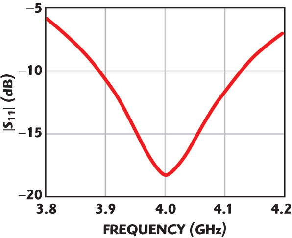
The structure is designed and simulated by a method of moment analysis using Agilent’s Momentum software. The simulated return loss of the designed antenna in a 50 ω system is shown in Figure 3. The achieved 10 dB return loss bandwidth is nearly 240 MHz, about the center frequency of 4.0 GHz and the gain of the patch is 9.05 dB. The variation of the return loss over frequency means that the impedance of the antenna is varying within the operating frequency range.
The simulated broadband impedance characteristics of the antenna show that the impedance is approximately 50 ω and demonstrate several resonance characteristics out-of-band.
The aperture dimensions are selected to minimize the back radiation in the operating frequency range.
Design and Simulation of the Integrated Amplifier with the Antenna
The amplifer is designed by transforming the dynamic input impedance of the antenna to the optimum load impedance of the power device, in order to achieve maximum output power and efficiency.

The layout of the matching circuits between the MGF2430 device and the antenna is shown in Figure 4. The nonlinear model of this device is used for harmonic balance analysis of the circuit and to design the matching networks. The matching circuits, with the associated biasing circutry, are accomodated on the side of the feed network to eliminate electromagnatic coupling between the antenna patch and the matching networks.
Double-stub matching is used for both the input and output-matching networks for broadband matching. Resistive loading, using a chip resistor R at the input of the device, is used to make the amplifier unconditionally stable over the broad frequency range.
The power amplifier integrated with the antenna is simulated using the co-simulation approach of Agilent’s ADS tool. Initially, a DC analysis is conducted to determine the gate bias voltage of the device for a 300 mA drain current at the drain supply voltage of 10 V.
Then a stability analysis is done and the value of the input loading resistor is determined to achieve unconditional stability of the amplifier.

The stability factor of the amplifier over the broad frequency range of 2 to 12 GHz is shown in Figure 5.
The stability factor, greater than one over the broad frequency range of the integrated amplifier, confirms that the amplifier will be stable irrespective of the several resonance impedance characteristics of the antenna.
Initially, a linear analysis is conducted, replacing the power device with its S-parameters, which is a fast method to determine the approximate matching networks of the amplifier to obtain the required gain and return losses of the integrated amplifier.
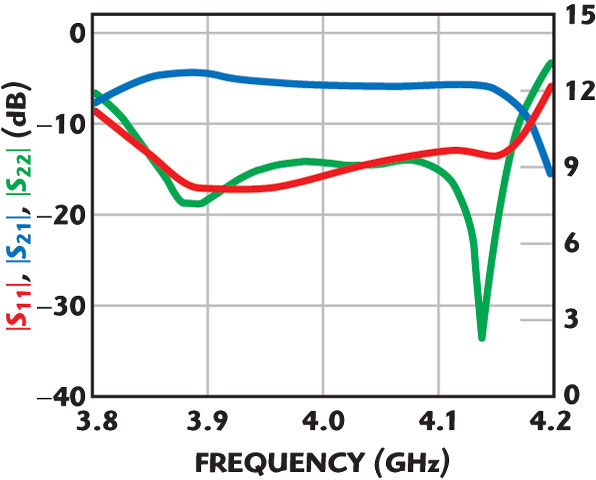
Figure 6 shows the small-signal S-parameters of the amplifier, considering that the antenna impedance is the output load of the amplifier.
The simulation shows that the small-signal gain of the amplifier is approximately 12 dB and both return losses are better than 12 dB over a frequency band of 300 MHz, around a center frequency of 4.0 GHz.
Finally a harmonic balance analysis is conducted, for the nonlinear analysis of the integrated amplifier using the nonlinear model of the power device.
The output-matching network is optimized for proper harmonic termination to achieve maximum output power from the amplifier.

The length and position of the stubs are determined for proper harmonic termination. The final output power as a function of input power is shown in Figure 7, at the 4.0 GHz center frequency.
The simulated output power, at the -2 dB gain compression point, is 32.2 dBm. It is also clear that the small-signal gain of the amplifier is nearly 12 dB, which agrees with the linear analysis.
The output-matching network is determined for maximum output power at the center frequency of 4.0 GHz. The variation of the output power (P2dB) over the frequency range of 300 MHz is nearly 1.6 dB, as shown in Figure 8.
The P2dB bandwidth is narrower than the small-signal gain bandwidth.

Conclusion
This article presents the design and analysis related issues of a solid-state power amplifier integrated with a planar antenna. It discusses the superiority of the aperture-coupled antenna structure to minimize the EM interaction between the antenna and the associated matching circuitry of the solid-state power amplifier. The design and simulation of an active antenna integrated with a power amplifier, using a type MGF2430 MESFET are presented, using harmonic balance analysis and an EM simulator simultaneously, to take care of the coupling between the antenna and matching circuitry and to address the out-of-band instability and nonlinear analysis of the power amplifier.
References
- R.A. York and Z.B. Popovic, Eds., Active and Quasi-optical Arrays for Solid-state Power Combining, John Wiley & Sons Inc., Hoboken, NJ, 1997.
- J.L.B. Walker, High Power GaAs FET Amplifier, Artech House Inc., Norwood, MA, 1993.
- D.M. Pozar, “A Microstrip Antenna Aperture Coupled to a Microstrip Line,” Electronics Letters, Vol. 21, January 1985, pp. 49–50.
- D.M. Pozar and S.D. Targonski, “Improved Coupling for Aperture-coupled Microstrip Antennas,” Electronics Letters, Vol. 27, No. 13, June 1991, pp. 127–129.
- R.N. Simons, R.Q. Lee and G.R. Lindamood, “New Coplanar Waveguide/Stripline Feed Network for Seven Path Hexagonal CP Subarray,” Electronics Letters, Vol. 27, No. 6, March 1991, pp. 533–535.
- R.N. Simons, R.Q. Lee and G.R. Lindamood, “Electromagnetic Coupling Between Coplanar Waveguide and Microstrip Antennas,” Microwave and Optical Technology Letters, Vol. 5, February 1992.
- W.J. Tseng and S.J. Chung, “Analysis and Application of a Two-port Aperture-coupled Microstrip Antenna,” IEEE Transactions on Microwave Theory and Techniques, Vol. 46, No. 5, May 1998, pp. 530–535.
- R.Q. Lee and R.N. Simons, “Coplanar Waveguide Aperture-coupled Microstrip Patch Antenna,” IEEE Microwave and Guided Wave Letters, Vol. 2 No. 4, April 1992, pp. 138–139.
- P.S. Hall, “Analysis of Radiation from Active Microstrip Antenna,” Electronics Letters, Vol. 2, January 1993, pp. 127–129.
- B. Robert, T. Razban and A. Papiernik, “Compact Amplifier Integration in Square Patch Antenna,” Electronics Letters, Vol. 28, September 1992, pp. 1808–1810.
- A.S. Andrenko, Y. Ikeda, M. Nakayama and O. Ishida, “Impedance Matching in Active Integrated Antenna Receiver Front-end Design,” IEEE Microwave and Guided Wave Letters, Vol. 10, No.1, January 2000, pp. 16–18.
- J. Lin and T. Itoh, “Active Integrated Antennas,” IEEE Transactions on Microwave Theory and Techniques, Vol. 42, No. 12, December 1994, pp. 2186–2194.
- Y. Chung, C.Y. Hang, S. Cai, Y. Qian, C.P. Wen, K.L. Wang and T. Itoh, “AlGaN/GaN HFET Power Amplifier Integrated with Microstrip Antenna for RF Front-end Applications,” IEEE Transactions on Microwave Theory and Techniques, Vol. 51, No. 2, February 2003, pp. 653–659.
- V. Radisic, Y. Qian and T. Itoh, “Novel Architectures for High Efficiency Amplifiers for Wireless Applications,” IEEE Transactions on Microwave Theory and Techniques, Vol. 46, No. 11, November 1998, pp. 1901–1909.
- V. Radisic, S.T. Chew, Y. Quin and T. Itoh, “High Efficiency Power Amplifier Integrated with Antenna,” IEEE Microwave and Guided Wave Letters, Vol. 7, No. 2, February 1997, pp. 39–41.
- W.R. Deal, V. Radisic, Y. Qian and T. Itoh, “Integrated-antenna Push-pull Power Amplifiers,” IEEE Transactions on Microwave Theory and Techniques, Vol. 47, No. 8, August 1999, pp. 1418–1425.
- C.Y. Hang, W.R. Deal, Y. Qian and T. Itoh, “High Efficiency Push-pull Power Amplifier Integrated with Quasi-Yagi Antenna,” IEEE Transactions on Microwave Theory and Techniques, Vol. 49, No. 6, August 2001, pp. 1155–1161.
- Y. Chung, C.Y. Hang, S. Cai, Y. Chen, W. Lee, C.P. Wen, K.L. Wang and T. Itoh, “Effects of Output Harmonic Termination on PAE and Output Power of AlGaN/GaN HEMT Power Amplifier,” IEEE Microwave and Wireless Components Letters, Vol. 12, No. 11, November 2002, pp. 421–423.
- S. Pajic and Z.B. Popovic, “An Efficient X-band 16-element Spatial Combiner of Switchable-mode Power Amplifiers,” IEEE Transactions on Microwave Theory and Techniques, Vol. 51, No. 7, July 2003, pp. 1863–1870.
- V. Radisic, Y. Quin and T. Itoh, “Class-F Power Amplifier Integrated with Circular Sector Microstrip Antenna,” 1997 IEEE MTT-S International Microwave Symposium Digest, Vol. 2, pp. 687–690.
- S. Gao, “High Efficiency Class-F RF/Microwave Power Amplifiers,” IEEE Microwave Magazine, Vol. 7, No. 1, February 2006, pp. 40–48.