
Phased arrays allow the electronic steering of an antenna beam in any direction and with high antenna gain by controlling the phase at each antenna element.
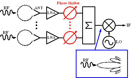
This beam steering technique is much more compact and much faster than mechanically steered arrays. Furthermore, phased arrays allow the creation of deep nulls in the radiation pattern to mitigate strong interference signals from several different directions (see Figure 1).
They have been in use since the 1950s in defense applications, but have seen limited use in commercial systems due to their relatively high cost. The main reason for the high cost of phased arrays is the complexity of the transmit/ receive (T/R) modules which contain low noise and power amplifiers, phase shifters, T/R switches, DC power control, and the necessary address decoders and memory latches for phase and gain setting for each module. Furthermore, T/R modules are hand-assembled using a combination of GaAs chips for microwave amplifiers and phase shifters, and CMOS electronics for digital control. A transmission-line based beamformer is also used to add all of the T/R modules together at the back-end of the array. All of this has basically resulted in very expensive phased arrays suitable only for defense applications.

The cost of phased arrays can be drastically reduced if several RF and digital functions are integrated together on a single chip. For a receive array suitable for wireless communications, for example, one can integrate the amplifiers, phase shifters, amplitude control and the 8:1 combining network, all on a single chip, using the latest SiGe/CMOS silicon RFICs. In the past few years, tremendous advances have occurred in SiGe and CMOS transistors and their integration technology. It is now possible to get 0.2 μm SiGe transistors with an ft of 120 to 150 GHz together with 0.18 mm CMOS transistors with an ft of 50 GHz in a standard BiCMOS process, such as the Jazz SiGe SBC18HX.1 A six-layer aluminum metal process embedded in an SiO2 dielectric medium is present above the transistors and allows for very dense RF and DC interconnects. The top metal layer is 3 mm-thick and is ideal for high Q inductors and low loss transmission lines. All of this makes the latest SiGe BiCMOS technology ideal for 2 to 60 GHz applications with excellent gain, noise figure and very high integration density.
Knowing this, an eight-element 6 to 18 GHz phased-array receiver on a single silicon chip was designed and tested (see Figures 2 and 3).

The phased-array chip was developed using the Jazz SiGe SBC18HX process. The RFIC chip contains eight RF inputs, followed by eight low noise amplifiers, eight phase shifters with at least four-bits of phase control, and an 8:1 active power combiner with very wide bandwidth (one RF output), together with all the digital functions needed to control the chip such as the address decoders for the individual eight elements, the memory latches for the phase settings, the clock enable functions to load the information on the chip and power regulators.
Furthermore, the chip can operate over a narrow bandwidth for communication systems, or over an instantaneous 12 GHz (6 to 18 GHz) bandwidth for EW or radar systems, while keeping its performance unchanged. Thus, solving one of the key barriers to complex phased-array fabrication.
One of the key elements in the design is the miniature 6 to 18 GHz phase shifter (see Figure 4). In this design, the input RF signal is first transformed into a differential signal using an active balun composed entirely of differential transistors, and the differential RF signal is then divided into in-phase (I) and quadrature (Q) signals using a passive I/Q network.
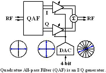
The I and Q signals are then added vectorially using a transistor summer circuit. This results in an output phase which can vary from 0° to 360° depending on the gain in the I and Q paths. This gain is set using a four-bit digital-to-analog circuit (DAC), with the input being the digital phase shift and the output being the analog current control for the I and Q paths. This circuit effectively results in a constant phase shift versus frequency and is therefore not a true-time delay circuit.
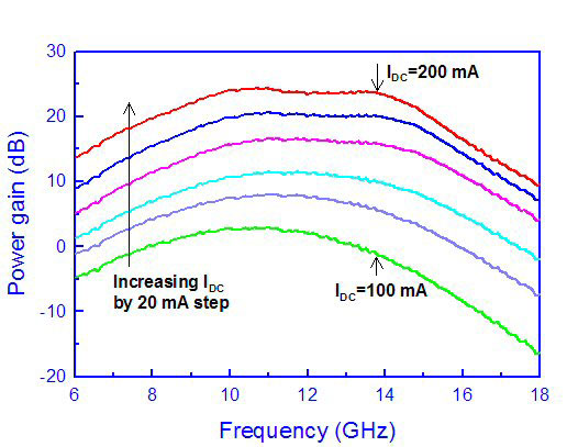
However, for an eight- or even a 16-element array, a constant phase shift is acceptable at the element level, and a TTD circuit is placed at the sub-array level for wideband beam control. Figures 5 and 6 show the measured gain and phase of a single element in the array. The measurements for the other seven elements are not shown and have virtually identical results. The chip is only 2.3 x 2.4 mm, consumes 100 to 200 mA of DC current from a 3.3 V power supply with an associated gain from 2 to 24 dB, and the phase response is nearly ideal from 0° (reference) to –337.5° (max. four-bit value).
The measured rms phase error, over the entire 6 to 18 GHz range, is less than 6° rms. This is an excellent result and shows a phase accuracy of nearly 6 bits. The measured noise figure is 6.2 ±0.2 dB at 12 GHz (not shown) over the entire 16 phase states.
The noise figure can be reduced in future designs to 2 to 3 dB especially for a 6 to 12 GHz operation. However, if a noise figure of 0.8 to 1.6 dB is required for applications such as satellite communications, then the chip must be preceded by GaAs low noise amplifiers.
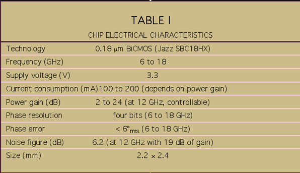
A summary of the chip’s electrical characteristics is presented in Table 1.
The application areas are in low cost phased arrays for mobile satellite systems, smart-antenna wireless systems for high data-rate communications, and, of course, defense systems such as radars and high bandwidth telecommunication links covering the X- to Ku-band frequency range.
The UCSD phased-array receiver is a disruptive element in the design of future phased-array systems and will replace at least eight GaAs chips. Furthermore, one can build 16-element or even 32-element phased arrays on a single silicon chip due to the high yield of BiCMOS technology. A 16-element 30 to 50 GHz phased-array transmitter is currently under development at UCSD.
Acknowledgments
This work was sponsored by the DARPA SMART (Scalable Millimeter-wave Array Technology) program under the direction of Mark Rosker and under a subcontract from Teledyne Scientific Corp., Thousand Oaks, CA. The phased-array chip was developed using the Jazz SiGe SBC18HX process.

 Kwangjin Koh received his BS degree in electronic engineering from Chung-Ang University, Korea, in 1999, and his MS degree in electrical engineering from the Korea Institute of Science and Technology (KAIST), Korea, in 2001. He is currently a PhD student at the University of California at San Diego. From 2001 to 2004, he worked at the Electronics and Telecommunications Research Institute (ETRI), Korea, where he was engaged in the research and development of RF and analog CMOS integrated circuits for wireless digital communications systems, such as WCDMA and WLAN 802.11a/b/g systems.
 Gabriel M. Rebeiz received his PhD degree from the California Institute of Technology in 1998. He is currently a professor of electrical engineering at the University of California at San Diego. He has contributed to planar mm-wave and terahertz antennas and imaging arrays from 1988 to 1998 and to the development of RF MEMS from 1996 to present.