
Module designs, and specifically handset power amplifier (PA) and front-end module (FEM) designs, are at a crossroads. Traditionally, the module has been an integration platform for discrete functional blocks enabled by considerable design margin, reasonable size and power constraints, and the luxury of predicted performance from cascaded analysis.
Although these issues may not be of concern in many current module designs, they soon will be, because increasing cost, complexity, integration and functionality will drive modules into realms of new design concerns. For years, going back to the Radiation Laboratory days, the majority of the time and effort invested in module design was spent on individual components.
Cascaded analysis by hand and then by spreadsheet, with the associated tradeoff among related blocks, left the majority of the module design task to finding either what combinations of individual block parametrics gave the highest yield, or what the various bonding or surface-mount technology (SMT) passive values were for “tuning in” marginal designs.
Later, with the advent of easy-to-use electromagnetic (EM) solvers or tools, some post-layout consideration was given to “design” of the module but, in reality, this was and continues to be more of a verification step.
With the explosion of the wireless market, all this is changing. Consumers want more features for the same price, vendors need more performance at a lower price and module designers are being pressured to deliver.
With more functionality going into a smaller footprint, the module can no longer be simply an integration platform. As performance requirements become more stringent, there is precious little margin to meet specifications, let alone design so that functional blocks can be merely cascaded; coupling among components must be minimized or even leveraged, if a PA/FEM module is to be successful in the marketplace.
Taking advantage of ever-shrinking market windows means that there may be time for a few design paths, but the days of doing iteratively endless module EM designs, followed by yet another printed circuit board (PCB) manufacturing run, are a thing of history.
In this article, a modern module design approach is explored, with emphasis on efficient design flow and effective methodology. The historical approach is reviewed and compared with a newer approach, looking at breaking down the previous barriers to actually designing modules by focusing on some very fundamental changes in design: multimedia design, co-simulation and early availability of EM. At a very high level, the flow is the same: partition the design, implement the individual functional blocks, integrate on the module and verify. But this is where the similarity ends, and the overall effect of the new design approach is to provide a higher degree of confidence in less design cycle time, ensuring that the module will be manufacturable in volume, cost-effective and will achieve its market window of opportunity.
Design Flow Overview
Traditional Approach
In the design flow used for years to design modules, the flow proceeds very serially, as shown in Figure 1.

From system partition to the individual design of multiple components (today normally limited to monolithic microwave integrated circuits (MMIC) or radio frequency ICs (RFIC)), to their layout, etc., electronic design automation (EDA) tools are underlying the flow, supporting pair-wise integration of adjacent steps.
This means that while the system and circuit simulation tools may have a translator to share schematics or a way to pass S-parameter files to each other, the circuit tools’ integration to layout does not provide a direct or obvious path to system simulation. The databases for the tools supporting any given step are distinct and, therefore, the data representing the design is spread out over multiple tools with no single database encompassing the entire design. Once the many IC components are designed and physically implemented, the module design proceeds. In this sub-flow, the “design” is actually driven by cramming all of the components into the mechanical outline defining the module package. Module “design” is normally done in a PCB layout tool for this reason, and interconnects consideration is relegated to a secondary, parasitic analysis role rather than a primary design role. On-module components, such as couplers, duplexers, or filters, may be designed using circuit tools, but then they are treated as isolated components similar to the ICs rather than as integrated elements. Within the last 10 years, EM tools have matured substantially, so that the circuit designer can intercept the PCB layout prior to manufacturing and begin tweaking the interconnects to back the design into acceptable performance.
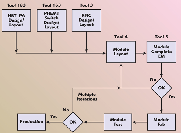
The design, as it were, is iterated between moving traces in the PCB, extracting a model for them with EM and simulating this model with behavioral or S-parameter models for the IC in a circuit tool. The ICs are not modified much beyond what their previously portioned performance dictates, except in rare circumstances. Once again, the pair-wise integration limitation of the supporting EDA software dictates that EM is done after layout and layout is done after circuit simulation, as shown in Figure 2.
There is no doubt that EM is an invaluable part of module design. Its proper use provides the most accurate models for the user’s design. For modules below 5 GHz or so, the majority of the design is done using RF lumped element design techniques, and the interconnects are better treated as parasitic and extracted rather than primary and modeled (presumably with microstrip or stripline models). However, the EM value in this flow is diminished and limited, because it is not accessible to the circuit designer during design and is used more to limit the parasitic impact of the module as opposed to leveraging the module to the designer’s advantage. Furthermore, the same can be said to be true of many parts of the flow. Individual IC designs are not mutually accessible, so there is limited opportunity to consider cascaded elements until a formal integration. In the case of the traditional flow, this integration is further hampered by the need to sometimes limit the modeling of ICs to S-parameter files and bonding diagrams rather than full, transistor-level descriptions and editable layouts. Opportunities early in the design flow to look at coupling issues, both IC-IC and IC-module, are nonexistent. As such, these can only be dealt with very late in the flow when time is short and re-design options are few.
Concurrent Approach
In order to look at coupling issues early in the design flow, it is necessary to reach down into the flow and break the barrier between the circuit designer and the EM solver.
At the same time, the same should be done for the system designer. By doing so, concurrency is enabled in the design flow, because all members of the electrical design team have access to the same data through an interface between the tools that support their task in the design flow. Such design flows are said to be concurrent. If this concurrency extends beyond the design media—the same tools and database being used for RFICs, MMICs and modules—the flow is said to be multimedia as well.
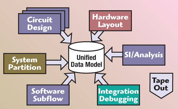
The key is to create a database or data model for the design that provides accessibility to the whole design for all participants through their step in the process. Furthermore, elements of the design, such as a microstrip, represent a single entry in the data model and each tool accesses the same entry for its use. So notions, such as cross-probing or schematic-driven layout, are no longer features written to integrate a set of tools, but rather are a fundamental consequence of the way the data is stored.
Such unifying databases have been implemented in spacecraft design,1 for example, and have enabled concurrent flows that reduce design time and increase the ability to handle complex designs. Databases of this sort exist for module design and enable a flow, as shown in Figure 3.
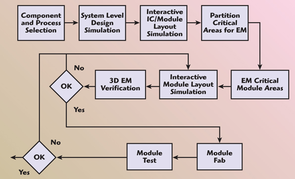
In this arrangement of tools, it is difficult to see how the flow plays itself out. In a word, it is flexible and can be anything from the arbitrary pinging back-and-forth to the highly serialized arrangement of the traditional approach. A more realistic approach can be seen in Figure 4.
The flow appears to be very serial; however, the key difference is that each step is actually very concurrent, as will be discussed later. How would this impact module design? Before the design flow can be considered at a very high level, with a step-by-step approach and seeing the radical effect concurrency can have on cycle time through this change in the module design process, it is important to look at how it changes a critical part of the module flow: the EM solver.
EM in Concurrent Design
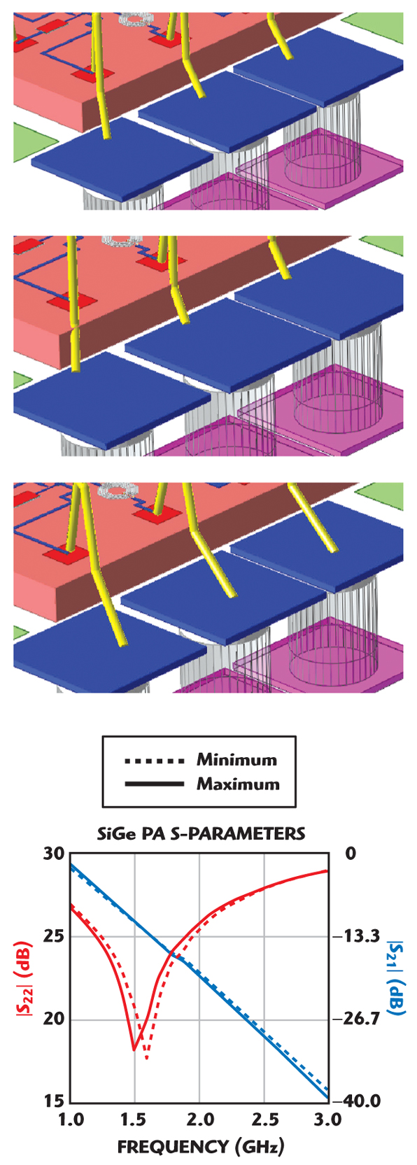
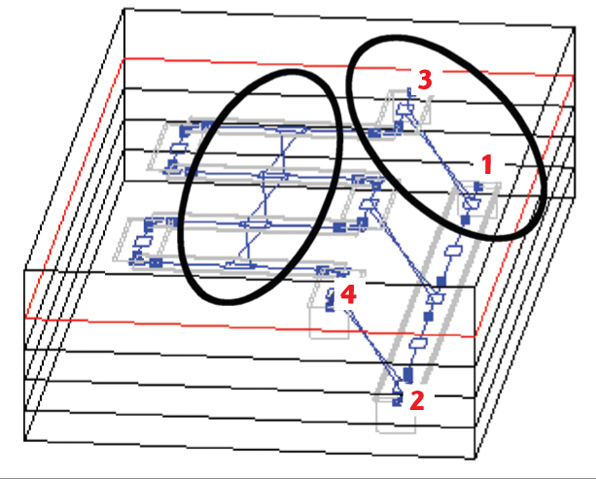
In the traditional flow, EM is only available post-layout and is de facto a module design step. This is very late to be using the most accurate means to model critical design elements. Conceptually, it would be desirable to have early access to it. Concurrent flows permit this by primarily removing the data barrier that exists among the tools. Since the layout and the EM are working from the same database, instead of an exported GDSII or DXF file, the EM can be driven directly from layout at any time without having to stop to export a file. The generated model is then automatically placed into the database as one of the possible electrical models for that portion of the design. This creates an interesting dynamic if the way in which the EM analysis is initiated is changed at this point. Imagine a circuit designer whose primary view of the design is the schematic, and now has direct access to the layout. By selecting larger and smaller sections of the layout, or parametrically tuning components—even interconnects—and then initiating the EM analysis through the circuit simulator, the designer has effectively moved EM into the circuit design flow and created a schematic-driven EM capability. The notion of parametric design and a concurrent database enables the designer to go even further. Rather than simply having parametric elements automatically create layout structures, as in the traditional flow’s schematic-driven layout, in a concurrent data model these elements could also use highly optimized EM solvers, built right into the models, to bring EM into the simulation and provide accessibility during real-time tuning, optimization, or statistical/yield analysis. Other methods rather than an explicit EM solver in the model are also possible.2 One example is bond wire modeling. Combining the parametric definition of bond wires, including multiple profiles, embedding dielectrics and material parameters, with layout cell generators and specialized EM solvers, three-dimensional (3D) EM simulation of bond wires can be driven by the schematic. This makes EM analysis of module-IC interconnects accessible very early in the design flow, ensuring that it is the same bond wire matrix that is in the layout and is sent to manufacturing. As shown in Figure 5, by parametrically varying the land location of the ground bonds for a silicon germanium (SiGe) PA at 1600 MHz between –50 to +150 mm from the nominal position, it can be seen that the performance shifts without explicit 3D EM.
For many interconnect structures, it is desirable to incrementally add parasitic and coupling effects early on, as the design progresses, considering them perhaps as innocuous shorts, then as simple distributed elements and finally as more and more complex coupling arrangements.
A new technology available in some software packages offers an intelligent net (iNet) capability, which enables a wire on the schematic to be routed on the layout and modeled using circuit elements.3 A new EM-like technology, circuit extraction (see Figure 6), can then group together these iNets and instead of doing time-consuming full-wave EM analysis, can effectively create a schematic model using distributed and coupled-line circuit elements. Circuit extract, when combined with EM-based models, brings the design full-circle, having effectively used schematics to kick-off EM, which in turn generates an EM analysis that produces a schematic with embedded-EM.
System Simulation
The module flow uses system simulation in three areas. Requirements flow-down is used very early in the process to partition the design into functional blocks. Behavioral models represent each component to be designed. Following this, the flow-down can be modified into a module verification mode by swapping out behavioral models for simulation-based ones.
These simulation-based models reuse the component schematics at the circuit level and automatically extract the needed system model through the single data model, even to the point that real-time tuning can be used as well as optimization of the system using circuit elements.
System simulation can be used in co-simulation with the circuit designs in a fashion similar to the module verification. Individual circuit designs can be inserted into test benches and the circuit schematic can be tuned or optimized for system performance.
For a PA module, for example, this could be error vector magnitude (EVM), adjacent channel power ratio (ACPR), or bit error rate (BER).
Circuit Design
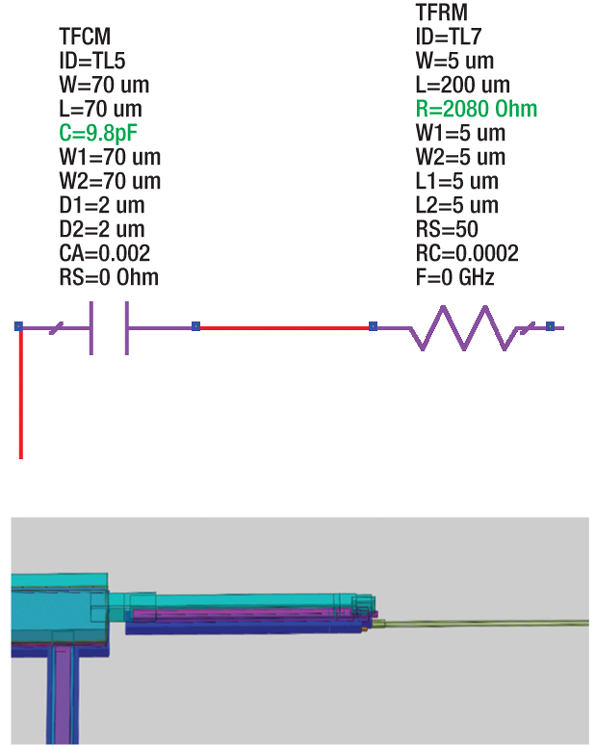
At some level, the designer must start by creating a schematic, doing some simulation and implementing with a little bit of layout. The value in the method under discussion in this article is that all these tasks are in the same tool, sharing the same database and the elements being placed in the schematic instantly have meaning in the other relevant steps in the process. Thus, the manipulation of the design can then switch to the layout, if that is the best way to manipulate the design, with the schematic automatically updating with each and every layout edit. EM can be implemented very early in the flow by using EM-based models or using EM to extract models directly from the layout under schematic control. This can also be done from the layout via the single data model because of the layout-schematic concurrency. This extends also to wires in the schematic. As shown in Figure 7, the wire in the schematic is automatically implemented knowing the precise via type that is needed—the connection to the capacitor is able to discriminate between cap top and bottom and can draw the appropriate via structure. This can then be extracted to circuit models, using circuit extract or S-parameters, using a full-wave EM solver. Because of the ease with which the circuit designer can introduce EM, it is relatively simple to incrementally add more and more peripheral metal to the EM until there is greater certainty of the desired performance. Because this incremental EM is done very early in the flow, it is much easier to make design changes when suggested by the EM results. As previously discussed, this can be done with system co-simulation as well, because the concurrent flow removes the overhead in the traditional flow of extracting behavioral models from the circuit tool and moving them to the system tool.
Module-IC Co-design
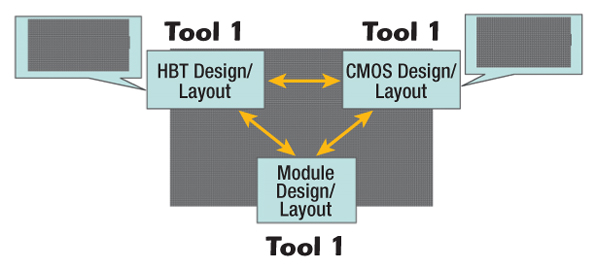
Once there is a semblance of a design for each of the components, the designer can now begin taking advantage of the concurrencies across the media. Figure 8, for example, shows that the heterojunction bipolar transistor (HBT) die can be individually designed in a concurrent fashion, as can a complementary metal oxide semiconductor (CMOS) or any other IC technology, in the same toolset, while simultaneously being co-designed with each other and the module itself.
The determining factor in where the concurrencies occur is the needs of the design and the creativity and problem solving of the engineer. The primary feature enabling this, beyond the concurrent data model, is the ability to load multiple process design kits (PDKs) for electrical and physical design.

For the example above, this means having multiple layer definitions and library elements for all three of these processes, as shown in Figure 9. Once the multiple PDKs are loaded, different IC-module co-design opportunities can be considered.
One obvious area is evaluating the tradeoff between a component on-die or on-module. It can be seen in Figure 10 that the original CMOS PA design calls for an inductor on the source of the second stage.
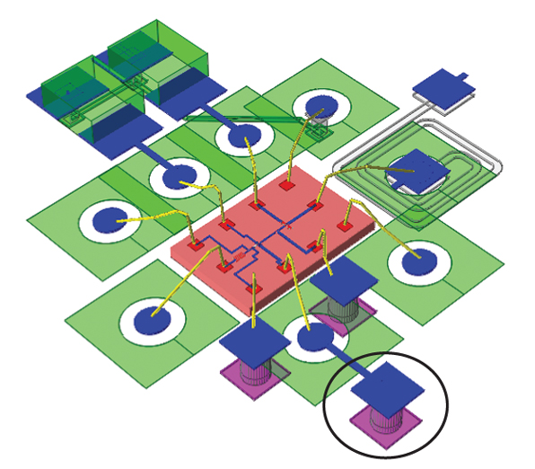
For die cost concerns, the designer may choose to explore moving this inductor, implemented as a spiral in the IC layout, to the module. Taking into account line lengths on the die and the module, as well as the layout-driven bond wire model with built-in EM, a module inductor can be synthesized that gives the equivalent effective inductance on-module as on-die, with a high degree of confidence in the results, as seen in the circled region in Figure 11.

Typically, this sort of analysis in the traditional flow would require the use of nearly all the tools (IC layout, PCB layout, circuit simulation and 3D EM), taking hours if not days to coordinate, simulate and analyze for a single iteration of the analysis. Here, in comparison, the whole process takes minutes, including optimizing the module line length. While it is true that as the module is finalized more and more direct current (DC), control and other routed lines will perturb the off-chip inductive solution, the critical design constraints for properly realizing the inductor through the layout-driven bond wire and the parameterized description of the inductive module line have been identified very early in the design process.
Good design practices, from this point forward in the flow, will enable the designer to incrementally examine how these other lines perturb the solution. In this way, a warning can be flagged and a second look taken at the module inductor as soon as it becomes an issue.
In contrast, in the traditional flow, there would not be any incremental knowledge of this, and the designer would not be able to see which “extra line” tipped the balance, since he/she would only be doing a full-up, complete module EM at the end of the complete, or nearly complete, module layout.
Also shown on top of the figure is a large matching inductor for the SiGe PA implemented off the chip. Co-designing this with the IC enables the designer to further minimize die size as well as performing sensitivity analysis for oscillations, before formally completing either the IC or the module design and layout. Once again, all of this is done very early in the flow, before formal or final layout of the module, enabling the SiGe PA designer and the module designer to have a dialog, if not do the outright design, using their preferred tools with a single database.
This can be extended further to IC-IC co-design. In this mode, the module can be considered immediately, or later on the interconnecting medium. As shown in Figure 12, the subject SiGe PA is now combined with a pseudomorphic high electron mobility transistor (PHEMT) PA via a coupler, presumably for feeding a common, broadband antenna.
Once sufficiently designed, the individual die can initially be directly combined or, later at the module level, used to consider the loading of one chip by another.

When this is done at the module level, the module interconnect source circuitry on one IC and load circuitry on the other IC become, instead of impediments, opportunities for performance improvement.
Thanks to the concurrency in the tools underlying the flow, the performance need not be just circuit, but also system. Complete implementation of the module can proceed once the (transistor-level) elemental descriptions of all the components are added. Co-design across all media boundaries is enabled or, for sufficiently mature and match-insensitive designs, just the module can be considered through design layout and unit verification.
Final Analysis and Verification
Once the module layout is completed, the designer “pops” back to the top level of the flow and does a final EM analysis and verification at the module level. The EM analysis may be full-module, but more likely than not, it will only be key areas of the module. The identification and partitioning of these areas were identified in the early parts of the IC, IC-module and IC-module-IC co-design segments with the incremental techniques discussed previously. Those areas, flagged as suspect or critical, will be analyzed one more time in this step and then combined with the transistor-level descriptions of the non-EM areas for final circuit- and system-level simulation and yield analysis. Any design rule check (DRC) and layout versus schematic (LVS) are done prior to generating data for IC fabrication, PCB manufacturing and module assembly.
Conclusion
Module design is no longer a matter of cascaded S-parameters and PCB layout. Design and market demands are forcing the module design focus to shift from component integration to a co-designed medium. The traditional design flow and underlying design tools are incapable of achieving this within the time-to-market requirements of modern PA/finite element method (FEM) products. Leveraging the lessons of concurrency from other areas, a set of tools and a flow based on a common database provides a low risk path to actually using the module to achieve greater performance, higher yield and lower cost.
Acknowledgment
The author wishes to acknowledge Dustin Hoekstra and Josh Moore of Applied Wave Research Inc. for their valuable contributions to this article.
References
- Courtesy of J.C. Sercel and ICS Associates, http://www.lsmd.caltech.edu/faq/ ICEpresentation.pdf.
- J.W. Bandler, Q.S. Cheng, S.A. Dakroury, A.S. Mohamed, M.H. Bakr, K. Madsen and J. Sondergaard, “Space Mapping: The State of the Art,” IEEE Transactions on Microwave Theory and Techniques, Vol. 52, No. 1, Part II, January 2004, pp. 337–361.
- M. Heimlich, et al., “Time-domain Interconnect Modeling for Pulsed and UWB Applications,” 2004 IEEE WAMICON.
 Michael Heimlich received his BSEE, MSEE and PhD EE degrees from Renssalear Polytechnic Institute. He is the microwave market segment director for Applied Wave Research Inc. (AWR), with responsibility for AWR’s flagship Microwave Office® design suite, as well as heading up the company’s university relations program. He has published papers in technical journals and proceedings in several important topical areas, including electro-optics, picosecond laser systems for broadband material diagnostics, MMIC and module design, and EDA tool integration. He holds a patent in the EDA tool integration area.