
High efficiency power amplifiers, combined with high linearity, have been very desirable. The Doherty amplifier is a technique for improving the efficiency at high output power back-off.1 Unfortunately, the Doherty amplifier has a poor intermodulation distortion (IMD) performance when the main and peaking amplifier’s signals are recombined at the output, using load modulation. This is because the peaking amplifier biasing mode is in class C, which generates high order IMD products.

In order to improve the linearity of a Doherty amplifier, a number of practical system-level techniques have been proposed: analog pre-distortion (APD), digital pre-distortion (DPD) and feed-forward linearization.2–4 Doherty amplification combined with analog pre-distortion has a simple operation, but its linear performance is limited. Digital pre-distortion and feed-forward linearization, when used in conjunction with a Doherty amplifier, provide good linearity. However, they have the disadvantage of bulky size and complex circuitry. The inherent linearity deterioration of a Doherty amplifier sets a threshold for achievable performance.
An alternative approach is the circuit-level linearization technique, based on the derivative superposition method (DSM), which utilizes multiple field effect transistors (FET) of different gate widths and gate biases.5–7 The DSM applications have been primarily used on MMIC power amplifiers.
This technique can be successfully applied to a Doherty amplifier. By comparing it with APD, which is a popular linearization technique, the DSM can achieve good linearity without the requirement of any external circuitry. Doherty amplifiers with improved efficiency and linearity have been reported recently.
8,9 The stringent linearity specifications required for WCDMA repeater or base station applications could not be met without an additional linearization technique. Therefore, the ACLR specifications of the Doherty amplifier require the use of both circuit- and system-level techniques simultaneously.

In this article, an optimized 20 W, high power and highly linear, digitally pre-distorted Doherty amplifier, which uses DSM, is proposed.
The linearity of the Doherty amplifier is first improved by using the DSM at the circuit-level. Digital pre-distortion is then utilized so that the Doherty amplifier is maximally optimized.
Analysis of a Linearized Doherty Amplifier
Derivative Superposition Structure
Figure 1 shows the configuration of a multiple FET combined amplifier, using the derivative superposition method. The main and N-auxiliary amplifiers are represented by their transconductance stages.

The main amplifier is identified as transistor M, which is biased by the gate voltage VM. The auxiliary amplifier N consists of a transistor MN, which is biased by the gate voltage VgsN. The gate biases are adjusted to compensate for the nonlinear characteristics of the main transistor.
The total output current of the multi-FET combination is expressed as

Where
Gm = transconductance, controlled by the gate-source bias Vgs
The DSM requires the summation of the derivatives of the various FET drain currents with respect to their gate voltages in order to achieve the desired transfer characteristics.
The nonlinear transconductance products generated by the main amplifier can be removed by independently compensating with the transconductance of the N-auxiliary amplifiers. This multiple FET amplifier can be applied to the Doherty structure, using two parallel LDMOS FETs.
Figure 2 shows the transfer function derivatives of a LDMOS FET model as a function of gate bias voltages. The third-order G3 term, which is of interest in power amplifiers, determines the in-band third-order intermodulation (IM3) distortion products. The G3 term can be observed to change slope and sign when the mode of operation moves between class AB and class C. In general, LDMOS FETs biased in class AB or class C mode have different transfer function derivatives versus gate bias and input voltage.
C. Fager, et al. have demonstrated the LDMOS FET transfer function derivatives for different classes of operation.10 The transfer function of a LDMOS FET can be modeled by a Taylor series expansion as follows:


where vin is an input voltage and the coefficients Gn are the transfer function derivatives of the nth-order IM products. In the design of a Doherty amplifier, the main amplifier is biased in the class AB mode and the peaking amplifier operates in the class C mode.
Linearization Optimization of the Doherty Amplifier Using Shunt Capacitors
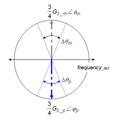
The proposed linearization principle of the Doherty amplifier is shown in Figure 3. The general principle is similar to utilizing the DSM, by adjusting two different gate biases. When the gain compression curve of the main class AB amplifier is compensated by the gain expansion curve of the peaking class C amplifier, a linear transfer function can be obtained. In order to understand the cancellation of the third-order term in the spectral domain, a two-tone input signal is applied


When a two-tone signal is injected into the main and peaking amplifier, the upper and lower sideband third-order IM terms (IM3) generated at the output of the main and peaking amplifiers can be calculated. In the memory-less amplifier model, the upper and lower sideband frequency components are symmetrical; therefore, the focus is on just the upper sideband. Using a Volterra series, the upper sideband third-order IM terms, 2w2–w1, of the main and peaking amplifier outputs at point A and A', in terms of Iout(vin), are given by

where H(w) is the nonlinear transfer function and G3m and G3p are the transconductances generated by the main and peaking amplifiers, respectively. Also, Φm and Φp are the phases of the third-order IM terms, which depend on G3m and G3p of the main and peaking amplifiers.
The adjustment of the two variable capacitors will result in the phase of the main and peaking amplifier outputs being a function of the frequency and capacitance. This can be respectively written as

Incorporating Equations 6 and 7 into Equations 4 and 5 at point B and B', the IM3 of the main and peaking amplifiers can be simply written as

where the IM3 magnitude of the main and peaking amplifiers, α3m and α3p, are

In order to reduce the IMD3 term, Equation 11 must be minimized


Accordingly, if the IM3 magnitudes of G3m and G3p are assumed to be the same, then the IM3 phase between the main and peaking amplifiers can be written as

Using Dqm and Dqp, the minimum IMD3 can be achieved, as shown in Figure 4.
Note that the third-order G3 terms of the class C biased peaking amplifier have a sign opposite to that of a class AB biased main amplifier.
Consequently, after the shunt capacitors values are adjusted, the gate bias of the main and peaking amplifiers and the input voltages could be properly optimized and the third-order IM products generated by the Doherty amplifier should be ideally cancelled out. The two critical parameters, which affect the minimization of the IMD3, include the gate bias and the output shunt capacitors.
Design and Simulation
A 20 W, high power Doherty amplifier is designed by using a push-pull packaged MRF6P21190 (Freescale’s LDMOS FET) with a P1dB of 190 W. The simulation of the Doherty circuit was performed using Agilent’s ADS software. Figure 5 shows the schematic diagram for the highly linear Doherty amplifier proposed in this article. One device is used as the main amplifier, while the other is the peaking amplifier. A 90° hybrid coupler is used to achieve the –90° phase shift at the peaking amplifier.
The peaking compensation lines and shunt capacitors are inserted so that both the efficiency and linearity of the Doherty amplifier are optimized. The output impedance, Zout, of the peaking amplifier was simulated to be 5.4 + j48.8 (Gout = 0.895 – 91.1°). By inserting the offset line, this point can be moved at 822+j260 (Gout = 0.895 – 2.0°). Therefore, this corresponds to an optimum high resistance, Ropt = 822 W. The high impedance of the peaking amplifier enables the output power of the main amplifier to be fully delivered to the load.

Thus, the offset line is necessary to prevent leakage power from the main amplifier into the peaking amplifier. The offset line has been shown to be very sensitive to the overall efficiency and linearity of Doherty amplifier.4
Figure 6 shows the simulated gain performance of the Doherty amplifier as a function of the gate bias of the main and peaking amplifiers. The bias dependent gain expansion characteristics of the peaking amplifier and also the gain compression characteristics of the main amplifier can be observed.
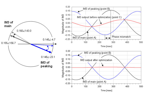
The designed Doherty amplifier has gate bias points of 2.88 V for the main amplifier and 2.07 V for the peaking amplifier. Figure 7 shows the simulated upper IM3 performance at points A, B and C.
Using shunt capacitors, the phase mismatch between the IM3 of the main amplifier and the IM3 of the peaking amplifier can be removed.
The IM3 of 0.160 – 143° for the main amplifier was moved to 0.155 – 156.7° and the IM3 of 0.145 – –4.7° for the peaking amplifier was simultaneously moved to 0.148 – –23.1°.

Therefore, the necessary 180° out of phase characteristic for a highly linear Doherty amplifier could be achieved. Figure 8 shows the simulated IM3 performance of a high power Doherty amplifier based on a two-tone input signal. The linearity performance of the Doherty amplifier was optimized using the gate biases, the offset lines and the shunt capacitors.
The IM3 performance of the Doherty amplifier, based on the optimization of shunt capacitors, could be improved by 10 dB in comparison to that of the Doherty amplifier before optimization. The corresponding power-added efficiency (PAE) was 24.8 percent at an average 20 W output power at 10 dB back-off.
Experimental Results
A Highly Linear Doherty Amplifier
LG.jpg)
A highly linear Doherty amplifier, using Freescale’s MRF6P21190HR6, was fabricated and measured at a center frequency of 2140 MHz using a single-tone signal, a two-tone signal and a single carrier WCDMA signal with a peak-to-average ratio of 9.8 dB.
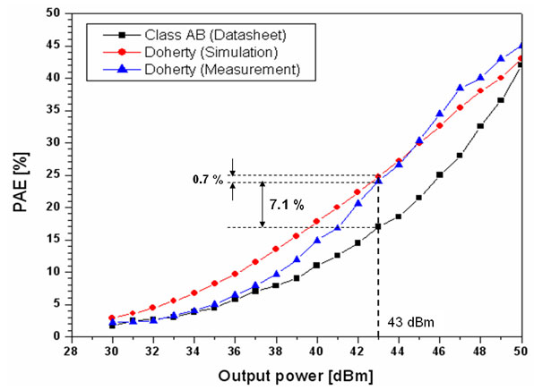
Figure 9 shows the measured efficiency characteristics of the highly linear Doherty amplifier compared to that of a Class AB amplifier datasheet11 and the simulated Doherty amplifier. The PAE of the Doherty amplifier could be improved by 7.1 percent compared to that of the Class AB amplifier at an average 20 W output power at 10 dB back-off.
LG.jpg)
Figure 10 shows the measured IM3 performance of the Doherty amplifier based on a two-tone input signal (2137.5 and 2145.5 MHz). Through optimization of the shunt capacitors (Cm = 0.6 pF and Cp = 0.4 pF), the IM3 performance of the Doherty amplifier improved 20 dB in comparison to that of the Doherty amplifier without shunt capacitors. These shunt capacitors must be selected with small values, which do not affect the matching circuit. At an average power of 43 dBm, the IM3 performance of the optimized Doherty amplifier achieved –51 dBc. At this point, the gate voltages of main and peaking amplifiers were +2.95 and +2.12 V, respectively. Figure 11 shows the IM3 performance of the Doherty amplifier as a function of output power. From the measured results, it is confirmed that an IM3 sweet-spot region with high linearity was obtained using the derivative superposition method in the Doherty structure. The measured results agree well with the simulation results.

Digitally Pre-distorted Doherty Amplifiers
Digital pre-distortion has been applied, using the indirect learning algorithm for a memory polynomial predistorter (PD), as shown in Figure 12. For the memory polynomial PD, the indirect learning using a recursive least square (RLS) algorithm was applied.12 The coefficients update equation can be expressed as

where a is the column vector for coefficients in the memory polynomial predistorter, e(n) is the error signal defined by


where y(n) is the row vector equal to [y(n) y(n)|y(n)| … y(n–1)|y(n–1)| …], and K(n) is the gain vector defined by

where λ is the forgetting factor, * represents the complex conjugate and the P(n) is updated as follows

Figure 13 shows the test bench set-up of the digitally pre-distorted Doherty amplifier. This test bench consists of a programmable signal generator (ESG E4438C) as a direct up-conversion path, a Doherty power amplifier (DPA), a vector signal analyzer (VSA 89641A) as a digital receiver to collect digital baseband samples from the output of the DPA, and a personal computer for digital signal processing. In the personal computer, Agilent ADS™ has been used for synchronizing both the samples from the signal analyzer and the samples at the output of the memory polynomial predistorter, that is, the original input for the first iteration, implementing the memory polynomial predistorter, and interfacing with the signal generator and after having both samples time-aligned, the indirect algorithm for parameter extraction has been implemented using Mathworks MATLAB.™
Figure 14 shows the measured WCDMA one-channel spectrum of the Doherty power amplifier with and without the inclusion of shunt capacitors as well as when digital pre-distortion is applied. At an output power of 20 W, the ACLR of an optimized Doherty amplifier with shunt capacitors improved by 16.7 dB compared to the Doherty amplifier before optimization, at the upper frequency offset of 2.5 MHz. By applying digital pre-distortion, a further ACLR improvement of 7.5 dB was obtained. The resultant WCDMA ACLR performance was –52.5 dBc at a 2.5 MHz frequency offset. The corresponding power-added efficiency was 24 percent. At this point, the gate voltages of the main and peaking amplifier are +2.93 and +2.17 V, respectively. Figure 15 shows the measured ACPR of the Doherty amplifier as function of output power. All the results were measured at ±2.5 MHz frequency offset from a center frequency of 2140 MHz. From the measured results, it is confirmed that the linearity of the Doherty amplifier can be improved by using the proposed optimization methodology.
Conclusion
An enhanced Doherty amplifier with highly optimized linearity using the derivative superposition method was designed and implemented for WCDMA repeater applications. Since DSM is a linearization technique based on the transconductance characteristics, it was found that the gain compression of the main amplifier, biased in class AB, can be compensated by combining it with the gain expansion of the peaking amplifier, biased in class C. In order to achieve IM3 cancellation in the Doherty structure, the gate biases of the main and peaking amplifiers must be optimized. The linearity optimization of the Doherty amplifier can be obtained by adjusting these important parameters: the offset lines, the gate biases and the shunt capacitors. A combination of digital pre-distortion along with the highly linear Doherty amplifier achieved an ACLR of –52.5 dBc at ±2.5 MHz offset frequency for a WCDMA signal. n
Acknowledgments
This research was supported by the Ministry of Information and Communication, Korea, under the Information Technology Research Center support program and supervised by the Institute of Information Technology Assessment.
References
- S.C. Cripps, RF Power Amplifier for Wireless Communications, Artech House Inc., Norwood, MA, 1999.
- T. Ogawa, T. Iwasaki, H. Maruyama, K. Horiguchi, M. Nakayama, Y. Ikeda and H. Kurebayashi, “High Efficiency Feed-forward Amplifier Using Complex Baseband Digital Predistortion Driven by CDMA Signals,” 2004 IEEE MTT-S International Microwave Symposium Digest, Vol. 2, pp. 537–540.
- Y. Zhao, M. Iwamoto, L.E. Larson and P.M. Asbeck, “Doherty Amplifier with DSP Control to Improve Performance in CDMA Operation,” 2003 IEEE MTT-S International Microwave Symposium Digest, Vol. 2, pp. 687–690.
- K.J. Cho, J.H. Kim and S.P. Stapleton, “A Highly Efficient Doherty Feed-forward Linear Power Amplifier for W-CDMA Base Station Applications,” IEEE Transactions on Microwave Theory and Techniques, Vol. 53, No. 1, January 2005,
pp. 292–300. - D.R. Webster, G. Ataei and D.G. Haigh “Low Distortion MMIC Power Amplifier Using a New Form of Derivative Superposition,” IEEE Transactions on Microwave Theory and Techniques, Vol. 49, No. 2, February 2001, pp. 328–332.
- J. Brinkhoff, A.E. Parker and M. Leung, “Baseband Impedance and Linearization of FET Circuits,” IEEE Transactions on Microwave Theory and Techniques, Vol. 51, No. 12, December 2003, pp. 2523–2530.
- V. Aparin and L.E. Larson, “Modified Derivative Superposition Method for Linearizing FET Low Noise Amplifiers,” IEEE Transactions on Microwave Theory and Techniques, Vol. 53, No. 2, February 2005, pp. 571–581.
- . K.J. Cho, I.H. Hwang, W.J. Kim, J.H. Kim and S.P. Shawn, “Linearity Optimization of a High Power Doherty Amplifier,” 2005 IEEE MTT-S International Microwave Symposium Digest,
pp. 1387–1390. - N. Srirattana, A. Raghavan, D. Heo, P.E. Allen and J. Laskar, “Analysis and Design of a High Efficiency Multistage Doherty Power Amplifier for Wireless Communications,” IEEE Transactions on Microwave Theory and Techniques, Vol. 53, No. 3, March 2005, pp. 852–860.
- C. Fager, J.C. Fedro, N.B. Carvalho and H. Zirath, “Prediction of IMD in LDMOS Transistor Amplifiers Using a New Large-signal Model,” IEEE Transactions on Microwave Theory and Techniques, Vol. 50, No. 12, December 2002,
pp. 2834–2842. - www.freescale.com.
- C. Eun and E.J. Powers, “A New Volterra Predistorter Based on the Indirect Learning Architecture,” IEEE Transactions on Signal Processing, Vol. 45, No. 1, January 2004, pp. 223–227.
- Y. Suzuki, S. Mizuta, T. Hirota and Y. Tamao, “Linearized Doherty Amplifier Using a New Digital Predistorter Compensating Frequency-dependent Intermodulation Distortion for Mobile Radio,” Proceedings of the 2004 Joint Conference of the 10th Asia-Pacific Conference on Communications, Vol. 2, pp. 558–562.
- . J. Sirois, S. Boumaiza, M. Helaoui, G. Brassard and F.M. Ghannouchi, “A Robust Modeling and Design Approach for Dynamically Loaded and Digitally Linearized Doherty Amplifiers,” IEEE Transactions on Microwave Theory and Techniques, Vol. 53, No. 9, September 2005,
pp. 2875–2882.
 Kyoung-Joon Cho received his BS degree in information and communication engineering from Anyang University, Anyang, Korea, in 1998, and his MS and PhD degrees in radio science and engineering from Kwangwoon University, Seoul, Korea, in 2000 and 2004, respectively. He joined the Simon Fraser University, BC, Canada, in September 2004, as a post-doctoral fellow in the school of engineering science, where he is involved with RFIC and MMIC power amplifier development. His research interests include MMIC/hybrid high efficiency power amplifier design and linearization techniques.
 Wan-Jong Kim received his BS and MS degrees in radio science and engineering from Kwangwoon University, Seoul, Korea, in 1999 and 2001, respectively. He has been pursuing his PhD degree in the school of engineering science, Simon Fraser University, BC, Canada, since 2003. His research interests include CFR techniques, RF/DSP design and digital linearization techniques.
 Shawn P. Stapleton received his BS, MS and PhD degrees, all in engineering, from Carleton University, Ottawa, Canada, in 1982, 1984 and 1988, respectively. He has been a professor in the school of engineering science at Simon Fraser University, BC, Canada, since 1988. His research interests include integrated RF/DSP applications for wireless communications, GaAs MMIC circuits and power amplifier linearization.
 Jong-Heon Kim received his BS degree in electronic communication engineering from Kwangwoon University, Seoul, Korea, in 1984, his MS degree in electronic engineering from Ruhr University, Bochum, Germany, in 1990, and his PhD degree in electronic engineering from Dortmund University, Dortmund, Germany, in 1994. He has been a professor in the department of radio science and engineering at Kwangwoon University since March 1995. His research interests include digital linearization of power amplifiers and transmitters, smart power amplifiers, and integrated RF/DSP design.
 Jin-Young Kim received his BS, MS and PhD degrees from the school of electrical engineering, Seoul National University, Seoul, Korea, in 1991, 1993 and 1998, respectively. He was a post-doctoral research fellow in the department of electrical engineering, Princeton University, NJ, from 1998 to 2000. He joined the faculty of the school of electronics engineering, Kwangwoon University, Seoul, Korea, in March 2001. His research interests include spread-spectrum communications for applications to terrestrial and satellite systems, modulation/demodulation, signal processing, packet radio network, optical communications, synchronization, channel coding, and detection and estimation theory.
 Byungje Lee received his BS degree in electronics engineering from Kyung-pook National University, Taegu, Korea, in 1988, and his MS and PhD degrees in electrical engineering from Southern Illinois University, Carbondale, IL, in 1994 and 1997, respectively. He has been a professor in the department of radio science and engineering at Kwangwoon University, Seoul, Korea, since 1998. His research interests include microwave antennas and numerical methods in electromagnetics, microwave passive, and active components and RFID systems.
 Jin-Joo Choi received his BS degree in physics from Seoul National University, Seoul, Korea, his MS degree in physics from Georgia State University, Atlanta, GA, and his PhD degree in nuclear engineering from the University of Michigan, Ann Arbor, MI, in 1983, 1985 and 1991, respectively. In 1997, he joined Kwangwoon University, Seoul, Korea, where he is currently an associate professor in the school of electronics engineering. His research interests include high power vacuum electronics and active and passive solid-state devices.
 Jong-Chul Lee received his BS and MS degrees in electronic engineering from Hanyang University, Seoul, Korea, in 1983 and 1985, respectively. He received his MS degree from Arizona State University, Tempe, AZ, in 1989, and his PhD degree from Texas A&M University, College Station, TX, in 1994. He joined the department of radio science and engineering of Kwangwoon University, Seoul, Korea, in 1996, where he is currently an associate professor. He also serves as project director at the ITRC RFIC Center, Kwangwoon University, which is funded by the Ministry of Information and Communication. His research interests include RF MEMS, RF applications of ferroelectric materials, millimeter-wave passive and active devices, MMIC and OEMIC.