
Semiconductor varactor diodes are commonly used throughout RF, microwave and millimeter-wave spectrums for a variety of applications,1,2 including the tuning of critical circuits such as voltage-controlled oscillators (VCO), filters, matching networks and phase-shifters in RFIC and MMIC circuits. However, semiconductor varactor diodes are limited in their applications by performance issues. Fundamentally, the quality factor (Q) for varactor diodes varies inversely to the tunable capacitance range of the diode. The Q suffers from the high series resistance of the varactor diode junction, which results in a decrease in Q when the diode capacitance is increased. Therefore, circuits requiring high Q values, such as high quality VCOs, do not rely solely upon varactors as their only source of capacitance. Varactors are often used in conjunction with off-chip discrete capacitors to maintain a combined minimum capacitance and Q. The addition of off-chip discrete components increases the size, complexity and cost of the circuits, so alternative solutions to this problem have been sought. One technology being investigated as a potential solution to this problem is RF-microelectromechanical system (RF-MEMS) variable capacitors (varactors).
RF-MEMS varactors and other components are being aggressively pursued throughout academia and industry, which has prompted the recent publication of reference books discussing the theory of design for these devices.3-5 Reviewing the literature reveals that numerous configurations for RF-MEMS varactors are being pursued.3-6 This article is intended as an introduction to the design of RF-MEMS varactors, so not every configuration can be discussed. Configurations can include tunable parallel plate capacitors, interdigital capacitors and variations of these concepts. The fundamental theory of design for RF-MEMS varactors is applicable to any of these concepts; however, this article discusses the design of tunable parallel plate capacitors (varactors) fabricated in the commercially available PolyMUMPs foundry.7
Parallel plate varactors fabricated in the PolyMUMPs foundry have been widely studied.8-14 The typical results obtained for these devices are a 2.1 pF device with a 38 percent capacitance variation and a Q of 9.3 at 1.9 GHz.13 It is quite evident that these results are limited in their applications by the small tuning range and low Q. Therefore, McGill University launched a research program to determine the tuning range and Q limitations for varactors fabricated in the PolyMUMPs foundry. The university was able to demonstrate varactors built in this foundry provide wide capacitance variations (49 to 433 percent) and high Q (Q = 25 to 90) values at 2.4 GHz, which is a significant improvement over previous results. This article provides the reader with the design procedure for the RF-MEMS varactors with these improved results.

The PolyMUMPs Foundry
The varactors explored by McGill University were fabricated in the PolyMUMPs foundry. It is important to understand the features of the process before discussing how to design devices in this foundry. The features of the PolyMUMPs process are illustrated in Figure 1, along with a limited set of the material properties for each layer of the process.7 The first layer is silicon nitride, which provides electrical isolation between the substrate and the surface micromachined structure being built on top of it. Next, the process provides three layers of polysilicon (Poly0, Poly1 and Poly2), which constitute the main structural layers. One gold layer is available, which can only be deposited on top of Poly2. Finally, the oxides provide two sacrificial layers that can be etched away, thereby releasing the micromechanically movable structures. The three polysilicon layers can be selectively joined using openings in the two oxide layers, or be insulated from one another using continuous sheets of oxide. This knowledge of the process is essential for exploring varactor configurations, and is particularly important for determining how movable and anchored structures can be fabricated.

Now that an elementary understanding of the PolyMUMPs process has been established, it is possible to begin looking at how parallel plate capacitors can be formed in this process. The process provides one metal layer, but a parallel plate capacitor is formed using two different conducting layers separated by a dielectric region. Therefore, the three conducting polysilicon layers must be used when fabricating capacitors in this process. A simple mechanical model of a varactor is described in Figure 2, where the capacitor is formed by a fixed plate and a movable plate. The fixed plate can be created using the conducting Poly0 layer, or by a stacked configuration of the Poly0 and Poly1 layers. The movable plate can only be formed by etching away one or more of the oxide layers to allow vertical movement. The movable plate can be formed by depositing gold on top of the Poly2 layer, or it can be formed from a stacked configuration of the gold, Poly2 and Poly1 layers. Essentially, there are three layer configurations possible for building varactors in the PolyMUMPs process, which are shown in Figure 3.

The three varactor configurations are mechanically tuned by changing the distance separating the plates. Therefore, the spacing between the plates must be mechanically controlled. The spacing between the plates can be adjusted in the PolyMUMPs process using electrostatic actuation3,10,15 as shown, or using thermal actuation.16,17 The use of electrostatic actuation dominates due to its inherent speed and the low actuation power required. Thermal actuators rely upon resistive heating to deform a structure as a function of its thermal coefficient of expansion. Thermal actuation is much slower than electrostatic actuation, and the power dissipated by resistive heating is much higher than that required for electrostatic actuation. Therefore, electrostatic was the only actuation concept considered.
Actuation occurs when an electrostatic force is created by applying a DC voltage between the capacitor electrodes. Increasing the DC voltage increases the electrostatic force between the electrodes, thereby displacing the movable plate toward the fixed plate.
Basic Principles for Operation and Design of MEMS Varactors
Considering the conceptual model of the MEMS varactor, when a control voltage (Vctl) is applied, the suspended plate moves toward the fixed plate until equilibrium is reached. Equilibrium occurs when the spring force (kx) equals the electrostatic force of the actuator

where
εair = dielectric constant of air
Aeff = effective area of the capacitor plates
d0 = distance between the plates when Vctl = 0
The tuning limits for electrostatic concepts are determined by the continuum of equilibrium states, which only exists when 0 <e; x <e; do/3 for the Type 1 varactor structure. Beyond this limit, the electrostatic force overcomes the spring force, resulting in contact between the two plates. This is known as the "pull-in effect."15 This sets a maximum theoretical capacitance value of 3Co/2 (Co being the capacitance for Vctl = 0). The theoretical change in capacitance for the Type 1 varactor is defined as:
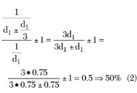
A Type 1 varactor was previously demonstrated in the PolyMUMPs process. The theoretical capacitance variation for this structure is 50 percent, but the maximum measured capacitance variation was limited to 38 percent.13
Type 2 describes the first possible implementation of the concept being explored here to extend the change in capacitance beyond 50 percent. It has been successfully demonstrated in other processes.18 It is based on the idea of using separate electrodes for actuation, while setting the biasing of the two plates forming the capacitor to the same DC potential. The actuation voltage is the voltage between the suspended plate and the Poly0 actuation electrodes, while the variable capacitance is formed between the Poly1 suspended plate and the Poly0 fixed plate. A continuum of equilibrium positions can now be obtained for displacements when x <e; d2/3. For d1 < d2, the maximum variation in d1 will therefore be larger than d1/3, leading to a capacitance variation larger than 3Co/2, corresponding to a change greater than 50 percent. It can quickly be seen from this example that the maximum variation depends upon the thickness of the layers used in the process. For the PolyMUMPs process, the maximum theoretical capacitance variation for the Type 2 structure is given by

A second variation of this concept can also be built using the PolyMUMPs process. It capitalizes on the specific layer thicknesses available in the process to further extend the capacitance as illustrated for Type 3. With this arrangement, d1 <e; d2/3, the theoretical capacitance variation for the varactor becomes infinitely wide.
Now that two new tuning implementations have been identified, the next step is to look at the mechanical aspects of the three varactors shown. It should be noted that these structures are represented using parallel planar surfaces. Undesirable non-planar or non-parallel surfaces can be created if the suspension beams or movable plates experience stress when fabricated. Therefore, the mechanical aspects of the varactor must be considered when designing this type of device. The suspension beams must be designed with the objective of minimizing the residual stresses, while also minimizing the resistive loss experienced by the RF current flowing across the beams. Residual stress in the beams can cause the movable plate of the varactor to be displaced, thereby preventing d1 from being exactly defined.
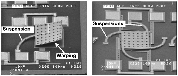
The residual stress problem is a result of the top plate being composed of two or three layers with different thermal expansion coefficients, namely polysilicon (Poly2 or Poly1 and Poly2) and gold.14 This can result in warping of the suspended plate, as illustrated in Figure 4. However, when multiple "C-shaped" suspension beams are used, they tend to absorb the stress by allowing horizontal rotation in the top plate.
Now that a rudimentary understanding of the effects of stress on a varactor has been established, it is equally important to understand how the materials of construction affect the Q of a varactor. The Q is one of the key electrical aspects of a varactor, which embodies the nature of the losses in the device.3,5 An examination of the parallel plate varactor structure under consideration reveals that it may be modeled using the lumped equivalent circuit shown in Figure 5. In general, for two-port applications, the Q is determined by both the series resistance of the suspension beams (Rseries) and the parasitic resistance from the bottom plate to ground (RBP). Since Q ∝ 1/Rseries, it is imperative to employ as thick a suspension metal coating as possible. Increasing the metal thickness minimizes the ohmic and skin-effect loss mechanisms for the varactor.5

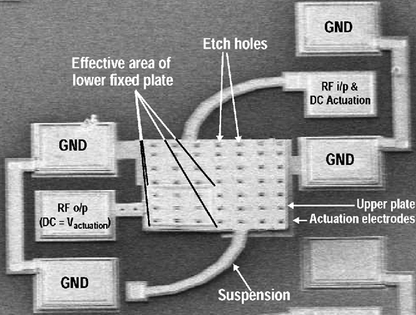
The loss mechanisms can be further understood using Figure 6, which shows a SEM photograph of a Type 3 varactor. The layout for this device was optimized to minimize losses. All suspensions connected to the upper moving plate are C-shaped, including the suspension carrying the input RF signal. This is necessary to minimize residual stress as discussed earlier. However, the longer signal path resulting from this shape also increases the series resistance losses. This is partially mitigated by covering the Poly2 suspension with a gold metal layer, resulting in a much lower total series resistance. The RF signal then crosses the capacitor to the fixed plate. The latter is connected to the output pad through a polysilicon conductor. This path is responsible for most of the losses in the device. First, the resistivity of Poly1 is relatively high when compared to that of gold. Second, extra losses are incurred due to the proximity of this conductor to the substrate. In order to minimize the resistive losses, the conductor to the output pad was made using Poly0 and Poly1 layers in parallel. Furthermore, the conductor was made as short and as wide as possible.
Now that the aspects of the design dealing with capacitance variation and Q limitations have been addressed, the design of the varactors may begin. The fringe free capacitance (Cfree) is determined using

where
ε' = relative dielectric constant
ε0 = dielectric constant of free space
A = area of the capacitor plate
d = distance separating the capacitor plates
The minimum and maximum fringe free capacitance values for the Type 1, 2 and 3 capacitors may be estimated through simulation and knowing the minimum and maximum values for d.
The capacitance of the plates must also include the effects of the fringing fields.3,19 For all the prototypes considered in this article, the fringing capacitances (few femto-Farads) were estimated to be much smaller compared to the main capacitances (few pico-Farads), and had a negligible effect at the frequency of interest (2.4 GHz). An accurate estimation of the total capacitance for geometrically complex varactor configurations can also be determined numerically using 3D codes such as Ansoft's HFSS,20 CST's Microwave Studio,21 or Flomeric's Micro-Stripes.22
The next item of concern for designing an electrostatically actuated varactor is determining the actuation and pull-in voltages for the structure. This was previously discussed with regard to establishing equilibrium between the electrostatic force and the spring force. The spring force for a varactor is determined by the resistance of the suspensions to mechanical deformation, while the electrostatic force is determined by the DC voltage applied across the area of the opposing actuator electrodes and the gap separating these electrodes. The actuator electrodes must be large enough to allow displacement of the movable plate at reasonable voltage levels for the intended application. Electromechanical analysis of complex structures like that shown is difficult to perform analytically, so tuning curves (capacitance versus voltage) are typically determined numerically. Tools such as ANSYS Multiphysics23 can analyze the deformation of a structure as a function of the actuator voltage, thereby eliminating the capacitance calculation errors introduced by analytic approximations.19
The final aspect to consider when designing an RF-MEMS varactor is the volume of the movable plate and suspensions. The size of the plate, suspensions and anchors, along with the mechanical features (materials of construction, stiffness, etc.) for these items, determines the mechanical resonance frequencies of a varactor structure. This aspect of the design determines the susceptibility of the device to vibration and other mechanical forces that can possibly interfere with the use of the device in a system. Once again, mechanically complex structures like that shown are difficult to model analytically, so numerical tools such as ANSYS Multiphysics are commonly used to determine their resonance frequencies, along with their susceptibility to externally applied periodic and aperiodic mechanical forces.
Measurement Results and Discussions
The structures were fabricated in the PolyMUMPs foundry to support and validate this study. As shown in the SEM photograph of the Type 3 varactor, etch holes in the top plate were used to allow removal of the sacrificial oxide during release. The large square patch in the picture delineates the effective area of the capacitor's lower fixed plate, while the remaining structural area was used for electrostatic actuation. As evident from the SEM photograph, the pad size is comparable to the effective area of the capacitor and must be de-embedded from the varactor measurements.24 The pad capacitance was measured to be 1.2 pF at 2.4 GHz.

Figure 7 shows the measured return loss S11 of a small varactor for minimum and maximum settings of Vctl. After de-embedding, the capacitance of the varactor varies from 0.16 to 0.68 pF, corresponding to change of 325 percent. The measured Q at 2.4 GHz under zero control voltage is 90. As the actuation voltage is increased, the top plate moves toward the bottom plate, causing the suspension carrying the input RF signal to stretch and become thinner; this results in an increase of its series resistance, and a decrease of the observed Q. For 100 percent tuning, the measured Q is 40, and for maximum tuning, drops to 25. For future designs, wider or parallel suspensions could be used to minimize this effect and maximize the Q. This will probably trade off with the need for higher actuation voltages. The elastic characteristics of the suspensions and the deflection of the top plate when an actuation voltage is applied were found to be the main limiting mechanisms for the maximum achievable capacitance range, compared to the theoretical infinite range.


Figure 8 shows a comparison of the capacitance characteristics of larger Type 1, 2 and 3 prototype devices versus activation voltage. Table 1 summarizes the characteristics of these devices, including their estimated and measured minimum capacitances when no activation voltage is applied. Note that all the expected capacitances are smaller than the measured values. It is speculated that the initial vertical gaps (d0) between the two capacitor plates were reduced as a result of the increased masses of the top plates due to the extra metal/Poly1 layers attached to them. This argument is supported by the fact that the discrepancy is higher for the Type 2 structure, which, unlike the other two structures, has both metal and Poly1 layers attached to Poly2. Modeling this structure with ANSYS Multiphysics before fabrication would have allowed this problem to be identified and solved during the design of these devices. For the Type 3 structure, the capacitance tuning range was 433 percent, for Vctl = 0 to 10 V. It is possible to obtain the same variation of capacitance using lower actuation voltages. This comes at the expense of a less robust mechanical design, making the device more sensitive to vibration. To cope with today's systems operating from low voltage batteries, voltage boosting circuitry, such as charge pumps, can be used.25 This is a common practice, especially feasible when no current is to be drawn by the device, which is the case for RF-MEMS switches and varactors.
A comparison of the performance achieved by the RF-MEMS structures evaluated by McGill University, state-of-the-art RF-MEMS and semiconductor varactors shows the very wide capacitance variation (49 to 433 percent) and high Qs (Q = 25-90) for the 2.4 GHz structures demonstrated by McGill University. The Q values for RF devices fabricated using the PolyMUMPs foundry were limited by the absence of a second metal layer. As mentioned earlier, the fixed plate of the varactors presented here are made of Poly1 in parallel with Poly0, which results in a relatively high series resistance. The low conductivity of the polysilicon also aggravates the skin-effect, even at the relatively low frequency of 2.4 GHz, resulting in further loss of power and Q degradation. Table 2 summarizes these results. Implementing these varactors in a technology offering more than one metal layer, such as the aluminum-based technology used by Young and Boser9 or the new MetalMUMPs process,26 is estimated to improve the Q by a factor of three to four, while benefiting from the very wide tuning range of the structures presented here.
This fundamental research project can be considered successful, since it was able to demonstrate construction techniques for varactors fabricated in PolyMUMPs that provide theoretical capacitance variations from a minimum of 50 percent to a maximum approaching infinity. Experimentally, these devices were able to provide a minimum capacitance variation of 49 percent, to a maximum of 433 percent. The knowledge gained from this study of the PolyMUMPs process can be used to optimize the characteristics of varactors being developed for commercial applications.

Conclusion
McGill University has demonstrated that RF-MEMS varactors fabricated in the PolyMUMPs foundry can be considered for commercial applications now that capacitance variation and Q limitations for devices fabricated in this foundry have been identified. Varactor designs were presented with performance exhibiting very wide capacitance ranges (49 to 433 percent) and high Q (Q = 25 to 90) values at 2.4 GHz. This academic research on varactors can assist newcomers to the RF-MEMS field in exploring the development of varactors for their specific applications.
References
1. I.D. Robertson, et al., RFIC and MMIC Design and Technology, Institute of Electrical Engineers, London, England, 2001.
2. T.H. Lee, The Design of CMOS Radio Frequency Integrated Circuits, Cambridge University Press, New York, NY 1998.
3. G.M. Rebeiz, RF-MEMS Theory, Design and Technology, John Wiley & Sons Inc., New York, NY 2003.
4. V.K. Varadan, K.J. Vinoy and K.A. Jose, RF-MEMS and Their Applications, John Wiley & Sons Inc., New York, NY 2003.
5. H.J. De Los Santos, RF-MEMS Circuit Design for Wireless Communications, Artech House Inc., Norwood, MA 2002.
6. H.J. De Los Santos, S.J. Cunningham, W.S. Best, A. Morris III and S.F. Bart, chapter entitled "Microwave MEMS and Micromachining" in the book edited by K. Chang, Handbook of RF/Microwave Components, John Wiley & Sons Inc., New York, NY 2003.
7. D. Koester, A. Cowen, R. Mahadevan and B. Hardy, PolyMUMPs Design Handbook Revision 8.0 (http://www.memsrus.com/mumps.pdf), MEMSCAP, Bernin, France, 2002.
8. D.J. Young and B.E. Boser, "A Micromachined Variable Capacitor for Monolithic Low Noise VCOs," Technical Digest, IEEE Solid-State Sensor and Actuator Workshop, Hilton Head Island, SC, June 1996, pp. 86-89.
9. D.J. Young and B.E. Boser, "A Micromachine-based RF Low Noise Voltage-controlled Oscillator," Proceedings of the IEEE 1997 Custom Integrated Circuits Conference, pp. 431-434.
10. A. Dec and K. Suyama, "Micromachined Varactor with Wide Tuning Range," Electronics Letters, Vol. 33, No. 5, May 1997, pp. 922-924.
11. A. Dec and K. Suyama, "Micromachined Electro-mechanically Tunable Capacitors and Their Applications to RFICs," IEEE Transactions on Microwave Theory and Techniques, Vol. 46, No. 12, December 1998, pp. 2587-2596.
12. A. Dec and K. Suyama, "A 2.4 GHz CMOS LC VCO Using Micromachined Variable Capacitors for Frequency Tuning," 1999 IEEE MTT-S International Symposium Digest, pp. 79-82.
13. A. Dec and K. Suyama, "A 1.9 GHz CMOS VCO with Micromachined Electromechanically Tunable Capacitors," IEEE Journal of Solid-State Circuits, Vol. 35, No. 8, August 2000, pp. 1231-1237.
14. A. Dec and K. Suyama, "Microwave MEMS-based Voltage-controlled Oscillators," IEEE Transactions on Microwave Theory and Techniques, Vol. 48, No. 11, November 2000, pp. 1943-1949.
15. S.D. Senturia, Microsystem Design, Kluwer Academic Publishers, Boston, MA 2001.
16. Z. Feng, H. Zhang, W. Zhang, B. Su, K. Gupta, V. Bright and Y. Lee, "MEMS-based Variable Capacitor for Millimeter-wave Applications," IEEE Solid-State Sensor and Actuator Workshop, June 2000, pp. 255-258.
17. D. Yan, "Mechanical Design and Modeling of MEMS Thermal Actuators for RF Applications," master of science thesis in mechanical engineering, University of Waterloo, Waterloo, Ontario, Canada, 2002.
18. J. Zou, C. Liu, J. Schutt-Aine, J. Chen and S.M. Kang, "Development of a Wide Tuning Range MEMS Tunable Capacitor for Wireless Communication Systems," Proceedings of the 2000 IEEE International Electron Device Meeting, pp. 17.2.1-17.2.4.
19. T.H. Lee, "Derivation of Fringing Correction (Danger, Will Robinson - Integrals, Cheese and a Breeze Ahead!)," EE414 Handout #9, Spring 2001, http://www.stanford.edu/class/ee414/Handout/HO9.pdf.
20. Ansoft's HFSS, http://www.ansoft.com/products/hf/hfss/.
21. CST's Microwave Studio, http://www.cst.de/.
22. Flomeric's Micro-Stripes, http://www.microstripes.com/.
23. ANSYS Multiphysics, http://www.ansys.com/ansys/mems/index.htm.
24. S.A. Wartenberg, RF Measurements of Die and Packages, Artech House Inc., Norwood, MA 2002.
25. D. Hong and M.N. El-Gamal, "Low Operating Voltage and Short Settling Time CMOS Charge Pump for MEMS Applications," 2003 International Symposium on Circuits and Systems (ISCAS), May 2003.
26. MetalMUMPs, http://www.memsrus.com/svcsmetal.html.
27. G. Ionis, A. Dec and K. Suyama, "Differential Multi-finger MEMS Tunable Capacitors for RF Integrated Circuits," 2002 IEEE International Microwave Symposium Digest, June 2002, pp. 345-348.
28. T. Soorapanth, C. Yue, D. Shaeffer, T. Lee and S. Wong, "Analysis and Optimization of Accumulation-mode Varactor for RFICs," VLSI Circuits Digest Technical Papers, 1998, pp. 32-33.
29. M. Innocent, P. Wambacq, S. Donnay, H. Tilmans, H. De Man and W. Sansen, "MEMS Variable Capacitor Versus MOS Variable Capacitor for a 5 GHz Voltage-controlled Oscillator," European Solid-State Circuits Conference (ESSCIRC 02), September 2002.
30. R. Castello, P. Erratico, S. Manzini and F. Svelto, "A 30% Tuning Range Varactor Compatible with Future Scaled Technologies," VLSI Circuits Digest Technical Papers, 1998, pp. 34-35.
31. W. Wong, P. Hui, Z. Chen, K. Shen, J. Lau, P. Chan and P. Ko, "A Wide Tuning Range Gated Varactor," IEEE Journal of Solid-State Circuits, May 2000, pp. 773-779.
Tommy K.K. Tsang received his B.Eng. and M.Eng. degrees with honours from the electrical and computer engineering department of McGill University, Montreal, Canada, in 1999 and 2002, respectively. He is a member of the RFIC group. His earlier research focused on low voltage bipolar and CMOS radio frequency low noise amplifiers for future wireless applications. Currently, he is working toward his PhD degree, focusing on novel high performance RFIC architectures and MEMS-based systems.
Mourad N. El-Gamal received his PhD degree from McGill University, Montreal, Canada, in 1998, where he is currently a faculty member and director of the RFIC group. In 2002, he was director of engineering then vice president of the wireless business unit of MEMSCAP, France. Earlier he worked for IBM and ALCATEL. He is the founder and president of InfiniteChips in Montreal, a mixed-signal IC consulting company. He is also a member of the technical advisory boards of other microelectronics companies. He is a member of the analog signal processing technical committee of the IEEE. He has received numerous teaching and research awards. He may be contacted via the Web at http://www.ece.mcgill.ca/academ/staff/mourad.html.
W. Scott Best received his PhD from the University of Utah, Salt Lake City, UT, as a member of the Air Force thermionic engineering program. He is currently the managing member of Triangle ElectroMagnetics LLC, a new company providing research and consulting services for the development and manufacturing of microwave devices and RF-MEMS, and providing consulting on full wave simulation of RF, microwave and millimeter-wave devices. From March 2001 until December 2002, he was a staff engineer for RF-MEMS at Coventor, Cary, NC, where he provided engineering support for external customers and contributed to the development of IP for Coventor. From February 1993 until February 2001, he was a research associate at DuPont CR&D, Wilmington, DE, where he developed microwave heating and microwave plasma processing techniques for materials manufactured by DuPont, and he contributed to internal RF-MEMS development programs.
Héctor J. De Los Santos received his PhD from the school of electrical engineering, Purdue University, West Lafayette, IN, in 1989. He is president and CTO of NanoMEMS Research LLC, Irvine, CA, a new company engaged in RF-MEMS and nanotechnology research, consulting and education, with activities aimed at discovering and exploiting fundamentally new devices and circuits enabled by these novel technologies.