
The rising demand for low cost, low power personal communication systems operating up to 6 GHz makes the integration of radio frequency subsystems on monolithic silicon substrates an attractive challenge. Deep sub-micron technology allows silicon CMOS or silicon-germanium (SiGe) integrated circuits (IC) to operate at frequencies well within the RF range.1 Thus, single-chip radio transceivers can be devised, integrating on the same substrate the RF front-end circuitry and the base band signal-processing sections. Great efforts are therefore being undertaken to design RF subsystems compatible with standard silicon processes.
Among the various difficulties related to this task, the on-chip integration of passive components (most notably, inductors) emerges as a critical bottleneck2 - high quality, low noise reactive devices are needed to build narrow-band filters, voltage-controlled oscillators, and low noise and power amplifiers. Inductors can easily be implemented by designing a spiral layout on a metal layer, but their behavior deviates from ideality for several reasons, such as the coil is built by patterning a thin layer of metal (usually aluminum) featuring a non-negligible resistance and/or the device lies close to a rather conductive silicon substrate. Hence, the coupling between substrate and spiral inductor is responsible for significant energy losses at high frequencies.
In the last few years, several techniques to circumvent the above problems have been proposed. M. Frei, et al.,3 showed that a modified CMOS substrate structure (inserting a 3 µm thick p+ layer between the p- starting material and the p- epitaxial layer) is capable of reducing the losses due to eddy currents. Another direction of research is related to the introduction of ferromagnetic materials to increase the inductance of the integrated device.4 Finally, non-standard Si technologies have been developed to realize inductors featuring state-of-the-art quality factors (up to 50).5 With reference to design issues, care should be exercised when considering integrated inductors6 - non-ideality must be accounted for at the circuit-design stage, which calls for a comprehensive description of the device behavior.7
In this article, a methodology for the rigorous analysis of silicon integrated spiral inductors is proposed. To this purpose, extensive use of a finite difference time domain (FDTD) simulator8 developed at the University of Perugia has been made. However, the proposed methodology can be applied with any other commercial FDTD software available to the readers. With this approach, very complicated structures can be described and a rigorous treatment of metal and substrate losses is possible. In particular, an analysis of the substrate conduction and displacement currents has been carried out to better understand the loss mechanisms. The accuracy of the simulation has been validated by fabricating a test structure in a standard 0.35 µm CMOS technology and comparing on-wafer measurements with the computations.

Structures
The basic characteristics of the fabricated structure are depicted in Figure 1 - a standard 0.35 µm CMOS process is adopted, featuring a lightly doped epitaxial layer on top of the heavily-doped silicon substrate and up to five metallization layers. The reference inductor has a square shape and consists of N = 2 turns. The size of the outer turn is D = 300 µm and the width of the metal trace is w = 9 µm, while the spacing between adjacent turns is s = 0.4 µm. Such a coil (called L1) is patterned on the top metal layer (M5), whereas the signal return path (that is the wire connecting the inner node) runs through the underlying layer (M4). Top metal layers are usually adopted for integrated inductors since they are the thickest layers available in a CMOS process, thus minimizing the series resistance. Moreover, they maximize the distance between the inductor and the silicon substrate, where eddy current losses occur.

The relevant process parameters of the inductor L1 are reported in Table 1. The device is associated with a suitable pad de-embedding structure - measurements have been carried out at the wafer level by means of an HP 8720 vector network analyzer and a probe station with ground-signal-ground (GSG) tips, featuring a 150 µm pitch. The pad dimensions are 100 x 100 µm.
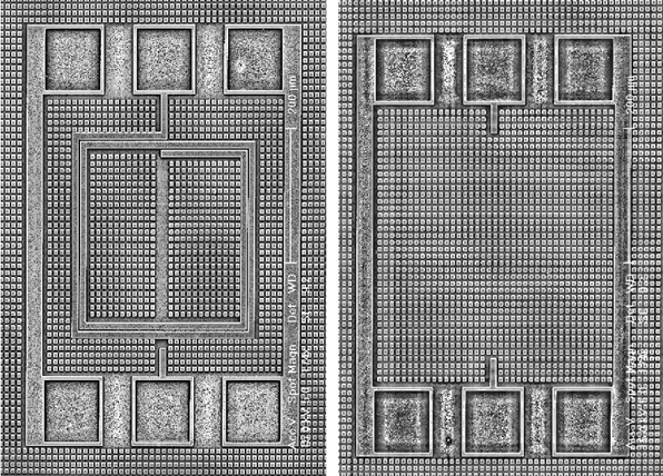
The short-open-load-thru (SOLT) calibration procedure has been performed by means of a standard calibration substrate. Then, using the integrated open (calibration) structure of Figure 2, a pad de-embedding procedure has been carried out. Following this procedure, the location of the electrical ports is set to 15 µm away from the inductor. In the remainder of the article, these locations will be referred to as "reference planes" T1 and T2. The adopted de-embedding technique, although very simple, does not completely remove the series parasitics from the ground lines. This means that, for a fair comparison with measurements, the simulated structure should resemble the experimental set-up.
Method of Analysis
The FDTD simulator described in Ciampolini, et al.,8 has been adopted for the analysis of CMOS integrated inductors. As is well known, this approach is based on the numerical, self-consistent solution of Maxwell's time-dependent curl equations. For this purpose, the space is divided in a finite number of elementary cells where electric and magnetic fields are mapped, while the time solution is obtained by an iterative scheme which evaluates the electric and magnetic field components at alternate half-time steps. Furthermore, lumped elements (resistors, generators, etc.) can be incorporated into such a framework. With reference to two-terminal devices, for example, the current-voltage equation I = f(V) that describes the element behavior is converted into a relationship J = g(E) between current density and electric field (associated to the elementary cell where the device is located). The latter current density term is inserted into Ampére's law to obtain an equation that describes the single-cell lumped element.
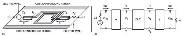
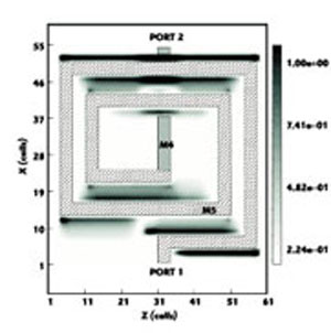
This simulation approach is illustrated in Figure 3, where only the metal layers of the device have been sketched. In particular, the central layout is the active signal path, while the two lateral lines (25 µm wide) are connected to the conductive silicon substrate underneath and form the ground returns. Lumped generators and loads have been used to provide a suitable excitation and termination to the analyzed structure. In this scheme a lumped generator (internal impedance Zg = 100 Ω) and a load (impedance Zl = 100 Ω) have been connected to two identical launching sections (length d = 100 µm) that feed the inductor under test. The resulting simulation environment can be considered as an approximation of the experimental set-up, based on GSG probe tips.
As shown in Appendix A, for the electrical characterization of an integrated inductor, the equivalent voltages and currents at the reference planes T1 and T2 must be determined. These quantities are not readily available from the FDTD simulation that, instead, provides voltages and currents at the lumped generator and load. Such values, however, can be used to evaluate the needed variables, under the condition that the electrical behavior of the launching sections is known.
For this purpose, the launching sections have been described by a transmission matrix [e]. With such a matrix, the electrical quantities at the reference planes can be expressed in terms of those directly measurable at the lumped elements. For example, V1 and I1 can be written as a function of V1m and I1m as
V1 = e11V1m + e12I1m
I1 = e21V1m + e22I1m (1)
Similarly, V2 and I2 can be obtained from V2m and I2m, using the same transmission matrix (the two launching sections are identical)
V2 = e11V2m + e12I2m
I2 = e21V2m + e22I2m (2)
The final step in this simulation technique is thus the evaluation of the transmission matrix [e]. To this purpose, a numerical algorithm referred to as a short-open-calibration (SOC) technique9 has been adopted. Such an algorithm is similar to the calibration usually performed with a vector network analyzer and requires two additional simulations of the launching sections.10 These simulations typically require only five percent of the CPU time needed for the analysis of the integrated inductor.
Validation
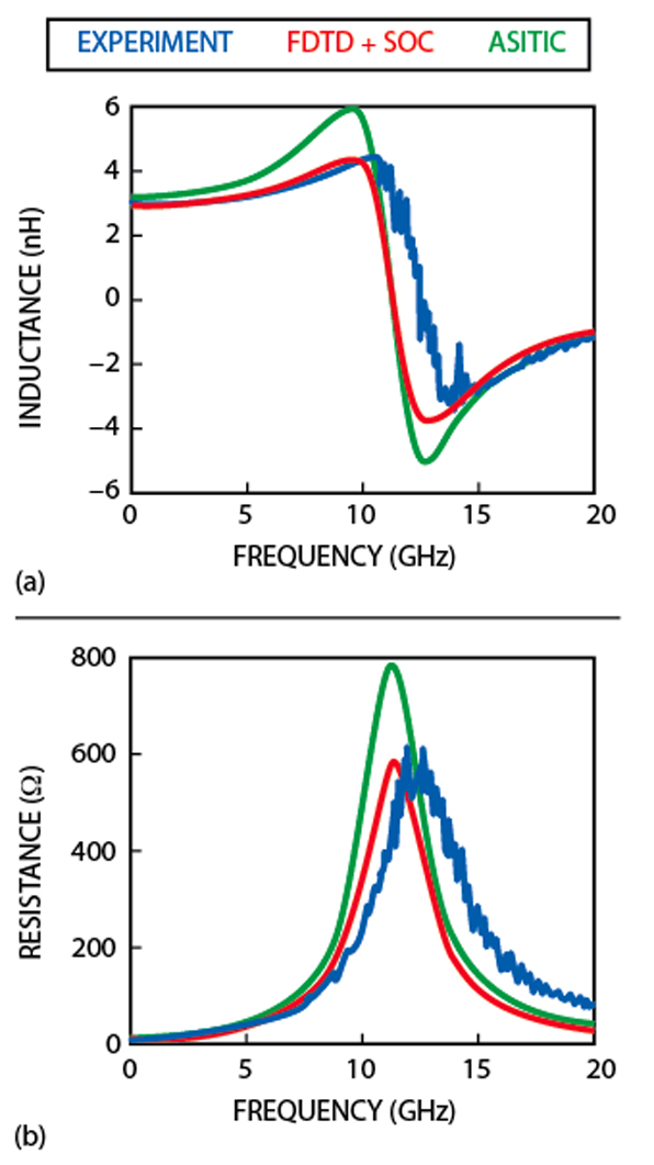
The inductor L1 has been used to validate the proposed methodology of analysis. The electrical characterization has been obtained with one of the two ports (that connected to the underpass) ideally short-circuited. Then, the input impedance of the resulting structure Zin has been evaluated starting either from the measurements or from the computations (both carried out on the two-port device). The same structure has also been analyzed using ASITIC,11,12 an inductor-dedicated software based on the combination of the Method of Moments with a sub-elements approach.
The obtained input inductance and resistance are shown in Figure 4 as a function of the frequency. In particular, the inductance is obtained as Im{Zin}/ω, while the resistance is just Re{Zin}.
A good agreement is obtained between the measured and simulated inductances at low frequency (approximately 3 nH). More precisely, the obtained values are within +6 percent (ASITIC) and the -6 percent (FDTD). The situation is different at high frequencies where the FDTD simulation seems to match better the experimental behavior. This is also confirmed by a better prediction of the peak values of both inductance and resistance. Finally, it must be noted that the self-resonance frequency is underestimated (by about 10 percent) by both simulators.

The quality factor Q = Im{Zin}/Re{Zin} can easily be obtained from the input impedance and has been derived from both simulators. The comparison with the measured data is shown in Figure 5. Again, it is apparent that the agreement obtained with the FDTD simulation is better than that achieved with ASITIC. This follows from a better modeling of the peak input resistance attainable with the numerical approach.
The cost of a better accuracy is, however, the greater computational effort needed for the FDTD analysis. The discrete computational domain used with such a simulator is composed by Nx x Ny x N = 41 x 81 x 77 cells with minimum dimension Δsmin = 0.2 µm. The time step has been chosen according to the Courant's criterion and is equal to Δtmax = 0.5 fs. The typical CPU time for 400000 time steps is approximately 7.5 hours on a AMD 1800 MHz desktop computer under the Windows operating system.
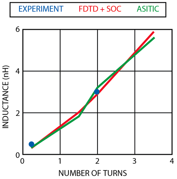
Finally, the validation has been extended to the cases of small and large inductance values. A device similar to L1 and featuring an external dimension of 300 µm has been simulated for different numbers of turns. The results have been compared with both ASITIC simulations and experimental measurements. The latter are available only for the structures implemented in this chip, namely the two-turn inductor described above and a 0.25 turn inductor (a direct connection between input and output ports). As shown in Figure 6, a good overall agreement between the two simulators is obtained for over a decade of inductance variation (from 0.3 nH up to approximately 6 nH).
Loss Analysis on a Reference Inductor
From the previous results, it is apparent that the Q factor of L1 is actually quite poor, and much lower than those customarily obtained with technologies more specifically suited for high frequency operation.5 In order to gain deeper understanding of the loss physics and to evaluate the spatial distribution of such losses at high frequencies, the displacement and conduction current fields (in the frequency domain) have been extracted from the simulations.
As the frequency increases, substrate effects tend to gain importance, prevailing close to the self-resonance region, where the inductor behavior suddenly turns into a capacitive one. At high frequencies, in fact, the current is no longer confined in the metal pattern and the relative importance of displacement currents increase as the frequency increases, as shown in Figure 7. Here, the displacement current component ∂DX/∂t computed at 10 GHz is shown and is particularly evident in the inter-turn gap. This points out the progressive coupling among adjacent legs of the spiral (a similar behavior is exhibited by the co-planar ∂DZ/∂t component, not shown here) that eventually results in a short circuit among nested turns.
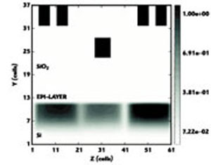
The coil, at increasing frequencies, tends to behave as a conductive plate, capacitively coupled with the substrate. This can be better appreciated by looking at a vertical cross-section of the device. The distribution of the displacement-current component ∂DY/∂t over a constant-x cross-section is reported in Figure 8. For the sake of clarity, this figure is not geometrically scaled, but a variable "stretching" coefficient (actually inversely related to the discretization cell-size) is applied to different regions in order to emphasize the qualitative behavior of distinct regions (explicitly labeled). A significant displacement current flows across the oxide layer. Most of this current turns into a conduction current as it penetrates deeply into the substrate, thus resulting in a large energy loss, which is responsible for a Q-factor degradation at high frequencies.
A further loss mechanism is due to the penetration of the magnetic flux generated by the coil into the silicon, which induces parasitic currents to circulate below the coil itself. Figure 9 makes such a statement evident. It refers to the x-component (which lays parallel to the silicon-oxide interface) of the conduction current, and clearly marks the eddy-current path.

The magnetic field has a further detrimental effect on the high frequency quality factor. In fact, the magnetic flux produced by the outer coil windings induces an opposite current at the inner turns, reducing the overall efficiency. Such an effect is responsible for an uneven current distribution within the strip cross-section which leads to a decrease of the effective strip section and thus to a frequency-dependent increase of the coil series resistance.
Conclusion
The numerical modeling of silicon integrated spiral inductors has been reviewed, based on the systematic application of an FDTD electromagnetic solver and of the SOC procedure. When taking into account actual fabrication parameters, severe performance limitations arise, mostly due to substrate losses. The good agreement obtained between measurements and simulations demonstrates that the developed virtual environment is a useful aid for the extraction of compact device models, suitable for commercial CAD packages.
References
1. T.P. Liu and E. Westerwick, "5 GHz CMOS Radio Transceiver Front-end Chipset," IEEE Journal of Solid-State Circuits, Vol. 35, No. 12, December 2000, pp. 1927-1933.
2. J.N. Burghartz, M. Soyuer and K.A. Jenkins, "Integrated RF Microwave Components in BiCMOS Technology," IEEE Transactions on Electronic Devices, Vol. 43, No. 9, September 1996, pp. 1559-1570.
3. M. Frei, "Integration of High Q Inductors in a Latch-up Resistant CMOS Technology," 1999 IEDM Digest, pp. 757-760.
4. M. Yamaguchi, M. Baba and K.I. Arai, "Sandwich-type Ferromagnetic RF Integrated Inductors," IEEE Transactions on Microwave Theory and Techniques, Vol. 49, No. 12, December 2001, pp. 2331-2335.
5. B. Piernas, K. Nishikawa, K. Kamogawa, T. Nakagawa and K. Araki, "High Q Factor Three-dimensional Inductors," IEEE Transactions on Microwave Theory and Techniques, Vol. 50, No. 8, August 2002, pp. 1942-1949.
6. J.N. Burghartz, M. Soyuer, C. Edelstein and Young, "RF Circuits Design Aspects of Spiral Inductors on Silicon," IEEE Journal of Solid-State Circuits, Vol. 33, No. 12, December 1998, pp. 2028-2034.
7. C.J. Chao, S.C. Wong, C.H. Kao, M.J. Chen, L.Y. Leu and K.Y. Chiu, "Characterization and Modeling of On-chip Spiral Inductors for Si RFICs," IEEE Transactions on Semiconductor Manufacturing, Vol. 15, No. 2, February 2002, pp. 19-29.
8. P. Ciampolini, P. Mezzanotte, L. Roselli and R. Sorrentino, "Accurate and Efficient Circuit Simulation with Lumped-element FDTD Technique," IEEE Transactions on Microwave Theory and Techniques, Vol. 44, No. 12, December 1996, pp. 2207-2215.
9. L. Zhu and K. Wu, "Unified Equivalent-circuit Model of Planar Discontinuities Suitable for Field Theory-based CAD and Optimization of M(H)MICs," IEEE Transactions on Microwave Theory and Techniques, Vol. 47, No. 9, September 1999, pp. 1589-1602.
10. F. Alimenti, V. Palazzari, P. Placidi, G. Stopponi, A. Scorzoni and L. Roselli, "Analysis of CMOS Interconnections Combining LE-FDTD and SOC Procedure," IEEE International Microwave Symposium Digest, Vol. 2, No. 6, June 2002, pp. 879-881.
11. A.M. Niknejad and R.G. Meyer, "Analysis, Design and Optimization of Spiral Inductors and Transformers for Si RF ICs," IEEE Journal of Solid-State Circuits, Vol. 33, No. 10, October 1998, pp. 1470-1481.
12. A.M. Niknejad and R.G. Meyer, "Analysis of Eddy-current Losses Over Conductive Substrates with Application to Monolithic Inductors and Transformers," IEEE Transactions on Microwave Theory and Techniques, Vol. 49, No. 1, January 2001, pp. 166-176.
 Federico Alimenti received his Laurea degree (cum laude) and his PhD degree in electronic engineering from the University of Perugia, Italy, in 1993 and 1997, respectively. In 1993, he held a scholarship from Daimler Benz Aerospace, Ulm, Germany. Since 2001, he has been a research assistant with the department of electronic and information engineering at the University of Perugia. His interests concern the modeling, design and realization of radio electronic circuits and wireless systems.
 Giovanni Stopponi received his Laurea degree (cum laude) and his PhD degree in electronic engineering from the University of Perugia, Italy, in 1995 and 2000, respectively. His research interests are mainly connected with the modeling of RF electronic circuits and devices, and with the development of digital apparatuses for wireless telemetry systems.
 Valeria Palazzari received her electronic engineering degree from the University of Perugia, Italy, in 2000, and is currently working toward her PhD degree in the department of electronic and information engineering at the same university. Her research interests are related to the modeling, design and testing of CMOS and SiGe integrated circuits for wireless systems.
 Pisana Placidi received her Laurea degree (cum laude) and her PhD degree in electronic engineering from the University of Perugia, Italy, in 1994 and 2000, respectively. Her research interests are mixed IC design and the modeling of HF electronic devices.
 Luca Roselli received his Laurea degree in electronic engineering from the University of Florence, Italy, in 1988. From 1988 to 1991, he worked at the University of Florence on SAW devices. In November 1991, he joined the Institute of Electronics at the University of Perugia, Italy, as a research assistant. In June 2000, he became an associate professor in applied electronics at the University of Perugia. That same year he founded WiS Srl, a spin-off company with which he is currently cooperating as a consultant. He is a reviewer for IEEE Microwave and Wireless Component Letters and IEEE Transactions on Microwave Theory and Techniques. He is also a member of the technical program committee of the International Microwave Symposium.
 Andrea Scorzoni earned his doctoral degree in electronics in 1989. Since 1983, he has been working at the CNR-Institute of Microelectronics and Microsystems (IMM, formerly LAMEL). From 1989 to 1998, he was responsible for several European scientific programs. From 1999 to 2001, he was coordinator of a national project on metal reliability in the frame of the CNR-MADESS II. He has been a professor of electronics at DIEI, University of Perugia, since 1998. His areas of interest include ohmic contact resistivity measurements and modeling for VLSI applications on silicon and silicon carbide, thermal modeling of sensors, design of microsystems, electromigration phenomena, reliability and degradation mechanisms of semiconductor devices, and solid-state, silicon-based, radiation sensors.
 Paolo Ciampolini graduated (cum laude) with a degree in electronic engineering in 1983. He received his PhD degree in electronics and computer sciences in 1989. From 1990 to 1992, he was with DEIS, University of Bologna, as a research assistant. From 1992 to 1998, he was an associate professor with the University of Perugia. He has been a professor of electronics in the department of information engineering at the University of Parma since 1998. His research interests include numerical modeling of semiconductor devices and circuits, solid-state silicon sensors, and digital system design.
