
Applied Wave Research (AWR) offers customization tools for particular processes to the Microwave Office (MWO) design environment. The tools needed to adapt a custom process to MWO are a text editor, Model Wizard, the Source Development Kit (SDK) and a MS Visual C++ compiler. The MWO plug-in Model Wizard is used to create the source code for custom models. Models can also be included in the Process Development Kit (PDK) as sets of S-parameter files. It is also possible to use existing MWO models.
The AWR SDK is needed by the C++ compiler to turn the source code for the models and layout cells into .dll files. A layout cell is implemented by built-in functions in the SDK. Various functions for different geometric shapes exist in the SDK. It is also possible to implement design rules in the source code. Layout cells and models are dynamically linked together by an .xml file in the PDK.
The PDK also contains a modified MWO shortcut, an initialization (.ini) file and a layer process definition (.lpf) file. If an MWO-228 license is available, a design rule check (DRC) file can be included in the PDK.
The .ini file specifies additional information, such as file paths to model and layout libraries, that needs to be added to the program on startup. File paths to the .lpf and .xml files are included in the .ini file. The modified MWO shortcut contains the path to the .ini file.1
The Component Library

The GMIC process has been adapted to MWO with the PDK. The GMIC process is a circuit technology, which has been under development at M/A-COM since 1985. GMIC provides a broad range of hybrid applications as well as efficient integration. GMIC is a robust fabrication technology capable of meeting the needs for high performance, complex microwave circuits in space, defense and other high reliability applications. M/A-COM offers different techniques of manufacturing GMIC applications. The adapted GMIC library to MWO uses the full glass process since it provides the highest performance and highest design flexibility.2
The GMIC substrate consists of a glass wafer laminated to a silicon wafer. The glass layer serves as the microstrip transmission medium and the silicon layer provides mechanical support and creates an integral carrier. Since glass has poor thermal conductivity, the silicon layer provides good heat transfer through the substrate. The composite microwave structure allows the use of standard silicon chemical processing, photolithographic and thin-film deposition techniques. By this method, it is possible to produce two layers of metallization, resistors, capacitors, inductors, conductors, air bridges and plated via-holes.2
The elements in Table 1 have been included in the GMIC component library. Dynamic layouts for all of the elements in the table have been constructed with the SDK. Model Wizard has been used to create models for pedestals, airbridge support pillars and probe points. The constructed models were aggregated from MWO schematics. For instance, the pedestal was modeled as a small resistor terminated to ground. The resistance values were found by simulating the pedestal in the High Frequency Structure Simulator (HFSS) from Ansoft. For other elements, the layouts have been linked together with existing MWO models.

The model for the Lange coupler has been modified by Model Wizard. The existing MWO model MLANGE has no parameters that specify the widths of the four feeding lines. In the modified model, the parameters for the four ports have been added to the existing model by Model Wizard. Values of the port widths do not affect the performance of the MWO model. The model for the Lange coupler is only used to generate layouts. To obtain as accurate a model as possible, the Lange coupler needs to be exported to an EM simulator.
Spiral Inductors
GMIC spiral inductors are implemented on the substrate as loops in one of the metallization layers. The inner turn is brought to the outside by a conductor crossing. A conductor crossing is constructed as a thin conductor with a dielectric layer above overlapped by an airbridge. The main motive for the dielectric layer is to prevent a short-circuit if the airbridge is crushed.3 The existing MWO model of a microstrip spiral inductor (MRINDSBR) has a parameter that defines the number of linear segments. A layout that takes consideration of this parameter has been constructed with the SDK.
The layout is valid between 5 and 27 linear segments. Of course, other parameters that define the geometry such as conductor width, outer dimensions and line spacing have also been taken into consideration. The layout has been linked together with the existing MWO model by the .xml library. Figure 1 show the layouts of the spiral inductor for different numbers of linear segments. It can be seen that the location of the bridge varies if the number of linear segments is changed.
The MWO model is only used to generate the layouts. Since a spiral inductor is dependant upon electric coupling, the structure needs to be simulated in an EM simulator.

When an arbitrary structure is exported from MWO to an EM simulator, it is possible to preset the 3D properties in the .lpf file. Figure 2 shows a 3D close-up view of the conductor crossing in a spiral inductor. The correct thicknesses of the layers that define the inductor have been specified in the .lpf file.
Thin-film Capacitors
A thin-film capacitor consists of two parallel metal plates separated by a dielectric layer. The bottom plate of the capacitor consists of a thin metal layer followed by a dielectric layer. The top plate of the capacitor consists of one of the metallization layers. An airbridge is used to interconnect the capacitor top-plate with the adjacent conductor.3 Thin-film capacitors are modeled by the existing MWO model TFCM. Figure 3 shows the created layouts of the thin-film capacitor. If the capacitor width exceeds the maximum allowed airbridge width, the airbridge configuration will be changed. Since airbridges are fabricated by a wet etch process, the airbridges cannot be as wide as possible. When a large airbridge is required, one or more slots must be included in the bridge to increase the span. Geometric properties, such as airbridge configuration and offsets of the layers that define the capacitor, are automatically fixed with the SDK.

To evaluate the Microwave Office model of a thin-film capacitor, the layout has been exported to HFSS from Ansoft. The HFSS simulation tool utilizes the finite element method (FEM) to solve Maxwell’s equations in the 3D structure. The results from HFSS showed that the accuracy of the MWO model is excellent in the frequency range from 5 to 15 GHz.
Design Rule Checking
If a MWO 228 license is available, design rule checking is possible to implement in the PDK. Design rules can be included as cell-based or polygon-based checking. Both types of design rule checking have been implemented in the GMIC component library.
The cell-based checks are implemented by overriding a checking function in the parameterized layout cell implementation. Design errors appear as dialog boxes when the check is performed. Rules, implemented as cell-based design rules, check only individual layouts. No interaction between adjacent elements is checked with this feature.4
Polygon-based design rules are implemented by built-in functions in MWO using a simple text editor. Rule checks for separation between layers, minimum area, overlap, minimum width, etc., exist in the set of functions. Polygon-based design rules work on arbitrary layout geometries in MWO. With this type of design rule check, it is possible to locate errors in dynamic layouts as well as in static GDSII layouts.4 Figure 4

shows a polygon-based design rule violation between two adjacent microstrip transmission lines. The spacing between the two lines is too small. As shown in the figure, a polygon-based design rule violation is visualized clearly in the MWO interface. Other types of polygon-based design errors, such as minimum area and overlap violations, are visualized in the same way. For more comprehensive knowledge about design rule checking, see Reference 4.
Design Example
The created GMIC component library was used in a master’s thesis called “Design of a Balanced X-band Low Noise Amplifier using a GMIC Process.”5 Some of the specified amplifier requirements are listed below:
• Frequency range: 8 to 12 GHz (X-band)
• S11 < –15 dB
• S21 > 8 dB
• S12 < –20 dB
• S22 < –15 dB
• NF < 3 dB
• P1dB > 5 dBm
• Gain variation within frequency range: ± 1 dB
• Current consumption: < 50 mA
• Supply voltage: +4 V
• The two amplifier branches should be biased from the same DC supply
.Figure 5 shows the circuit schematic of the amplifier. The selected transistor for the amplifier was the Excelics EPA018A high efficiency heterojunction power FET. The EPA018A has a noise figure of 0.75 dB and an associated gain of 12.5 dB at 12 GHz. S-parameter files measured under specific bias conditions were supplied by the manufacturer. The large-signal model was represented as a Curtice-Ettenburg model in MWO. The large-signal model parameters were provided by the manufacturer.6

According to the design specification, the two amplifier branches should be biased from the same DC supply. This problem was circumvented with a DC network, which consists of radio frequency chokes (RFC) and blocking capacitors. The constructed network divides the current contributed by the supply equally between both amplifier branches.
The resistors connected to the transistor sources limit the currents through the transistors and give the required bias settings on the gates. Both transistors have been biased with +4 V and 25 mA. An amplifier with this bias settings results in a compromise between class A and class AB operation. The requirements for unconditional stability were satisfied by placing shunt resistors at the inputs and outputs.
Series resistors have also been placed at the outputs. According to basic amplifier theory, resistors are preferably placed on the transistor output since the noise caused by a resistor at the input results in amplified noise. No combination without a shunt resistor at the input was found to satisfy the unconditional stability requirements. The resistors at the inputs are also required for the DC bias settings.
To compensate the gain variations, input and output matching networks (IMN and OMN) have been included in the design. The main disadvantage with this technique is the poor impedance match. Since the gain is decreased at some frequencies, more power is reflected. A good impedance match is achieved if two identical amplifier stages are placed between two 3 dB 90° hybrids.
The incident power wave on the input is equally divided in magnitude but with a phase shift of 90° between the input ports of the two amplifier branches. The output 3 dB 90° hybrid combines the output signals from the two amplifiers by introducing an additional 90° phase shift, thus bringing them in phase again. Lange couplers were used in the design, since they are the smallest microstrip realization of a 3 dB 90° hybrid and can be fabricated with the GMIC process. Signals reflected from the input and output ports of the two amplifier branches are summed together and dissipated in the 50 Ω terminations of the Lange couplers.7
Lange Coupler
A Lange coupler has been constructed with the adapted component library of MWO. The Lange coupler consists of microstrip segments interconnected by cross-unders, that is, the same type of interconnections as in the spiral inductors.

The MWO model was only used to generate layouts of the Lange coupler. The feeding lines were designed with a characteristic impedance of 50 Ω. Optimal dimensions were found by simulating the structure in HFSS. With optimal dimensions, the transmission S-parameters S21 and S31 shown in Figure 6 were obtained.
The results show that the transmission parameters S21 and S31 are both –3 dB, that is, the magnitude of the incident power on port 1 is equally divided between ports 2 and 3. Another important feature of the Lange coupler is the phase difference of 90° between ports 2 and 3. Since the length of the Lange coupler is λ/4 at 10 GHz, phase differences of 90° at 8 GHz and approximately 92° at 12 GHz were achieved. The 2° difference between the frequencies 8 and 12 GHz can be neglected.
The Balanced Amplifier

Figure 7 shows the layout of the complete balanced X-band low noise amplifier. The outer dimensions of the amplifier are 9 by 9 mm. All the layout work has been accomplished with the adapted GMIC component library to MWO. Optimal dimensions of the input and output matching networks were found by using the optimization utility in MWO.
The input-matching network suppresses high frequencies and the output-matching network suppresses low frequencies. High gain at low frequencies can start undesired oscillations in the amplifier; the output-matching network improves the stability.
Tuning options have been included in the resistor networks and in the input and output matching networks. For instance, the source resistance value can be changed if the airbridge interconnection in the middle network branch is moved. To facilitate manual bonding, airbridge support pillars have been added on both sides of the conductor gaps in the resistor networks.
The tuning options in the matching networks were implemented in the same way. The 50 Ω resistors terminating the Lange couplers were designed with the same width as the feeding lines. A 50 Ω resistor with smaller dimensions than the implemented resistor required an impedance transformer to minimize the discontinuity introduced at the interface of the Lange coupler. The additional length added by the impedance transformer reduced the performance of the balanced amplifier, since the phases of the reflected signals were changed in the 50 Ω terminations.
The motive for the RFC (the spiral inductor) and the blocking capacitor placed on the lower amplifier branch is to ensure that the output ports of the two branches are seeing equal impedances. According to the balanced amplifier performance, the amplifier has been designed to be as symmetrical as possible.
Simulations

Table 2 contains some of the simulated results of the balanced amplifier. As shown, all of the amplifier requirements have been satisfied. According to the design specification, the 1 dB compression point P1dB should be greater than 5 dBm. The amplifier delivers linear output powers up to approximately 13 dBm. One of the reasons for this feature is the balanced amplifier configuration. A balanced amplifier delivers twice the output power of a single amplifier branch.
The poor impedance matches in the single branch amplifiers were heavily reduced by introducing the Lange couplers in the design. As shown in the table, S11 and S22 have magnitudes less than –22 and –28 dB, respectively.
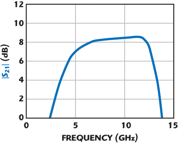
As shown in Figure 8, the gain requirements have been satisfied. The flat and broadband frequency response was achieved by the frequency compensated matching networks placed on the inputs and outputs of the amplifier branches.
Conclusion
With a basic knowledge in C++ programming, it is possible to adapt a custom process to MWO with the PDK. Instead of designing microwave circuits with manually implemented static layouts, the PDK is a convenient way to make dynamic layouts. If a custom process is adapted to MWO, the development time when designing microwave circuits in the specific process will be reduced. Another important advantage with the PDK is that design errors will almost be eliminated. When the design work of the balanced low noise amplifier was finished, the layout was submitted to the manufacturer M/A-COM. The layout was reviewed for manufacturability only. Since no design errors were found, the adaptation of the GMIC process to MWO was considered successful.
Acknowledgments
The authors gratefully acknowledge Mats Eriksson at MTT AB for providing the Microwave Office 228 license and the PDK tools. Rikard Eliasson would also like to express appreciation to his colleagues within the Microwave and Proximity Fuze Technology Development Group at SAAB Bofors Dynamics AB in Linköping, Sweden, for their supervision and support.
References
1. Applied Wave Research, “AWR PDK Training.zip,” Various PDK Presentation Materials from MTT AB, May 2005.
2. A. Buckle and A. Paffard, “GMIC-Glass Microwave Integrated Circuit, a Wafer Level Technology for Improved Performance of Microwave Components and Subsystems,” M/A-COM Ltd., ESA WPP-063, May 1993.
3. L. Christie, “GMIC Process Overview,” Tyco Electronics UK Ltd., M/A-COM Division, 2003-10-31 (restricted property of M/A-COM).
4. Applied Wave Research, Microwave Office User Guide, V5.5, July 2002.
5. R. Eliasson, “Design of a Balanced X-band Low Noise Amplifier Using a GMIC Process,” MSc Thesis, LITH-ITN-ED-EX-06/007-SE, February 2006.
6. Excelics Semiconductors Inc., “Data Sheet for the Transistor EPA018A,” www. excelics.com/p018a.pdf, accessed 21st September 2005.
7. G. Gonzalez, Microwave Transistor Amplifiers-Analysis and Design, Second Edition, Prentice Hall, Upper Saddle River, NJ, 1997.
| |