
The market demand for increased functionality, higher reliability and performance within ever shrinking form factors has placed new demands on designers of high performance designs. The convergence of RF, analog and digital systems within the same design and package now requires engineers to consider coupling effects that were heretofore negligible. This article will highlight the new challenges today’s designers encounter and present new solutions using case studies from collaborations with the world’s leading technology companies.

Zoltan Cendes is founder and chairman of Ansoft Corp., Pittsburgh, PA.
One trend that has become absolute is the convergence of RF, analog and digital systems in the same design and package. An example of such a device is the SCH-B570 phone introduced by Samsung Electronics. The Samsung phone has an 8 GB hard drive capable of recording 16 movies, picture-in-picture functionality, a 2 Mp camera, GPS functionality and an MP3 player capable of storing 1600 files.
To achieve the goal of high performance in small size at low power consumption, system-on-chip (SoC), system-in-package (SiP) and package-on-package (PoP) designs have become prevalent design configurations. These platforms combine RF, analog and digital components to enable efficient integration of computing, multimedia and communications functions. Cost/performance targets drive the integration of ICs, SoCs and SiPs onto low cost printed circuit boards. Process migration to 65 nm and below, multiple stacking packages, high performance CPUs and multi-band antenna topologies are at the heart of mobile products and technology strategies worldwide.
The challenges posed by RF/analog/digital integration require the integration of electronic design automation (EDA) software as well. In years past, it was sufficient to use one EDA vendor’s tool to perform harmonic balance circuit simulation on an oscillator, power amplifier or mixer, another vendor’s time domain circuit simulation tool to compute the transient response of a data converter or PLL, and still a third vendor’s electromagnetic simulation tool to compute the effect of interactions in the interconnects. With tightly integrated systems, chip/package/board co-design is required. The days when RF, analog and digital designs were performed in isolation are nearing an end.
New Challenges in High Performance, Integrated Design
The first challenge faced in high performance design is that of simulating in both the time and frequency domains and integrating RF metrics (such as gain, phase noise and insertion loss) with analog metrics (such as eye diagrams and skew rates). For consistency and accuracy, it is important to use the same simulator to perform both frequency domain harmonic balance analysis and time domain Spice simulation. The circuit models deployed should not vary across the frequency domain and time domain, ensuring results across analysis domains are the same. Ansoft’s circuit simulator Nexxim“ provides designers with the ability to accurately simulate in both domains and successfully integrates the disparate harmonic balance and Spice simulation technologies.
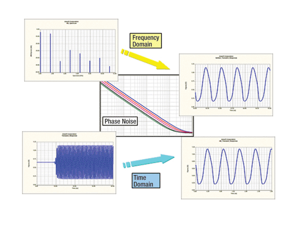
Consider the design of a voltage-controlled oscillator for an ultra-wideband radio. It is important to perform a harmonic balance simulation of this circuit to determine its oscillation frequencies and to compute the phase noise. In addition, it is important to determine the transient response of the circuit at start-up. If two different simulators are used to perform these two types of analysis, a discrepancy between the results may occur. However, Nexxim uses a single set of models and fundamental numerical constructs in both types of analysis. As shown in (Figure 1,). the result obtained from the harmonic balance simulation is the same as that obtained using a long (long enough to achieve steady state) transient simulation.
The second challenge faced in next generation design is substrate coupling due to the higher levels of device integration. Substrate coupling effects and other parasitics are often described in the frequency domain while the operating frequencies within a radio circuit are defined by the carrier frequency, the local oscillator and all tones (harmonics and intermodulation) generated by circuit nonlinearities. For high frequency designs, simulation in the frequency domain is more efficient and faster than in the time domain. This efficiency and speed provide a distinct advantage for harmonic balance over other techniques in the analysis of broadband radio blocks.
In the past two decades, harmonic balance algorithms have worked well for RF board and MMIC applications containing device counts ranging up to a few hundred transistors. However, next generation RFICs incorporate thousands of active device and tens of thousands of post-layout parasitics and operate with many independent and harmonically related tones. Traditional harmonic balance solvers are incapable of handling the large number of devices and circuit harmonics. Nexxim incorporates proprietary preconditioning schemes and iterative solution techniques that reduce the computational complexity and memory requirements for harmonic balance analysis, enabling the analysis of even larger circuits.

To examine the capabilities of this new iterative solver for large circuits, the RFIC differential IQ mixer, shown in (Figure 2,) was simulated with post-layout parasitics included in the simulation. The total component count was 95,127 of which approximately 1500 were MOSFETs and 90,000 elements were extracted RC parasitic elements. The mixer was driven by two independent RF signals which included two harmonics each and the local oscillator tone including one harmonic. This problem size proved too large for conventional harmonic balance simulation, which fails to converge. Nexxim’s algorithmic innovations allowed the same problem to be solved in just 42 minutes.
Full-wave Accurate PCB Simulations
Next generation electronics often contain PCBs and packages of immense complexity. To determine the electromagnetic interactions of these structures, a new technology was developed that exploits their predominantly planar composition. The software tool is called SIwave and it provides fast package and PCB analysis for large complex structures by taking advantage of the orthogonality of planar modes and transmission line modes. These orthogonal modes allow the software to significantly reduce the problem size from what it would be if the same structure were analyzed using a full 3D solver. SIwave solves a wave equation based upon the finite element method between the planes, providing a full-wave solution that is accurate until non-TEM parallel plate modes begin to propagate (that occurs when the plane-to-plane spacing approaches half a wavelength; about 300 GHz for FR4 with 10-mil spacing).
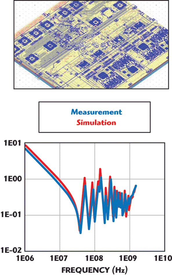
SIwave extracts parasitic parameters (S, Y and Z), displays 3D electromagnetic fields and generates broadband SPICE and/or S-parameter models from layout data that is directly imported from industry standard PCB and package layout tools. The resulting data allows engineers to characterize resonances, reflections and coupling between traces and power/ground planes for boards such as the 30 by 40 cm, 26 layer PCB with 6500 nets shown in (Figure 3).. This particular board resulted in a problem size of 1.75 million unknowns yet was solved in less than 20 minutes. The simulation closely matches measured results from 1 MHz to 10 GHz.
Frequency-based Models in the Time Domain
In addition to handling larger problems, today’s circuit simulation requires the flexibility to handle models from multiple vendors at varying levels of abstraction. This involves the ability to natively parse a variety of descriptive languages (SPICE, Verilog, VHDL, IBIS, Touchstone…), the ability to integrate and simulate circuits and sub-circuits described at the transistor level up to behavioral level as well as the ability to include the parasitics associated with passive interconnects and components operating at high frequencies. These parasitics are typically represented as static S-parameters from electromagnetic (EM) simulation or from measurement or as dynamic S-parameters via parametric EM/circuit co-simulation. One growing concern with S-parameters is that they are frequency domain models that must often be used in transient time domain simulations. The simple solution would seem to be to apply an inverse FFT, impulse response or convolution technique to the S-parameters to make them suitable for transient analysis. However, these approaches often raise problems with causality, non-passivity, lengthy simulation run times and in some cases wrong results or a failed simulation altogether.
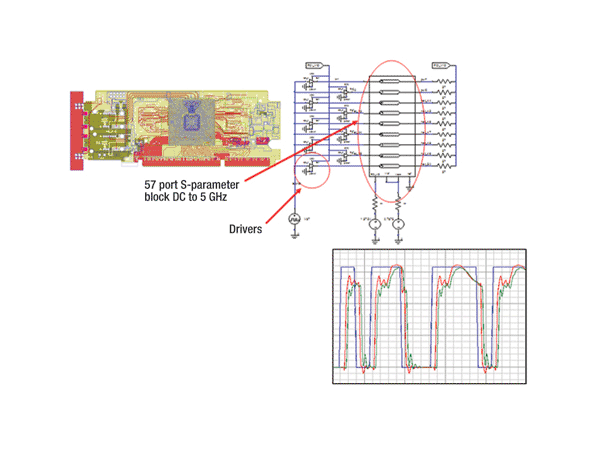
Nexxim utilizes a state space approach based on a pole-residue fit to the frequency domain data. By applying this formulation to only stable poles, causality is preserved. The model-order reduction also includes a passivity enforcement algorithm that may be set by the designer. This proprietary pole-residue fitting algorithm leads to extremely efficient transient simulations by reducing the problem to a simple first-order differential equation enabling fast and accurate simulation results. The advantage of the state space approach is evident in the investigation of simultaneous switching noise on the high speed PCB shown in Figure 4. The board, modeled as a 57 port S-parameter block from DC to 5 GHz, was terminated with 18 IBIS drivers and 50 &Omega loads. The transient simulation from t = 0 to t = 50 ns took just over five minutes to complete. Automatic caching of the pole-residue fitting data re-applies the results of the fitting operation for an unchanged passive network to further speed subsequent time domain analyses.
Today’s technology leaders often demand greater simulation accuracy than what IBIS models provide. However, the complexity and size of such a problem using silicon or transistor-level drivers is beyond the limits of traditional circuit simulation methods. Nexxim was designed to satisfy this unique requirement. In (Figure 5,)
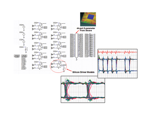
the complete design is solved with transistor level accuracy and frequency dependant layout effects. The design includes an extracted, 44 port S-parameter package model, and the complete circuit with 148,000 MOSFETs, 1.7 million capacitors and 500,000 resistors. Designers may now fully verify much larger designs with full-wave and transistor level accuracy to minimize surprises after tape-out. Further system simulation accuracy may be achieved when silicon or transistor-level drivers are incorporated instead of IBIS behavioral models. In the past, the complexity and size of such a problem was beyond the limits of existing circuit simulation. Today, Nexxim has the capacity to address the complete driver/receiver/channel chain as is demonstrated in the example. This level of design verification will be critical to eliminating repeated board, package and/or IC design cycles.
Chip/Package/Board Co-design
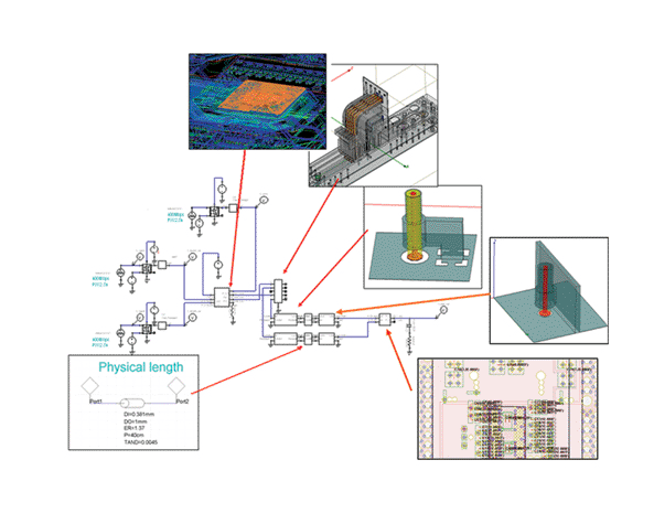
To illustrate the next generation of integrated design environment, consider the example of an advanced DDR2 test bench. This system consists of a driver circuit and package, a main printed circuit board, an interface board, several connectors, a coaxial cable and the test board itself. The system operates using a double data rate (DDR) channel in which logic triggers under both the rise and fall of each signal. The DDR standard calls for operational clock rates from 133 to 200 MHz, DDR2 from 266 to 400 MHz and DDR3 from 533 to 800 MHz. To maintain data integrity as clock speeds increase, full channel analysis is required from the main board through the connectors to the test board and back again.
The high level schematic of the memory test system is shown in (Figure 6). In this schematic, the various elements represent the main components of the system. The main board and the test board are simulated in SIwave to compute the input impedance of the boards as a function of frequency. The frequency dependent S-parameter block is then used in Nexxim circuit simulation.
The connector and interface board is simulated in the 3D electromagnetic field simulator HFSS.™ The parasitics of the interface board to coaxial cable connection as well as the coax to test board are computed by using the 3D parameter extraction tool Q3D Extractor.“ The coaxial cable itself is modeled using analytical models in Ansoft Designer.“ Finally, a test probe model from the data sheet is included to ensure a one-to-one correspondence between the measurement parameters and the simulation parameters.
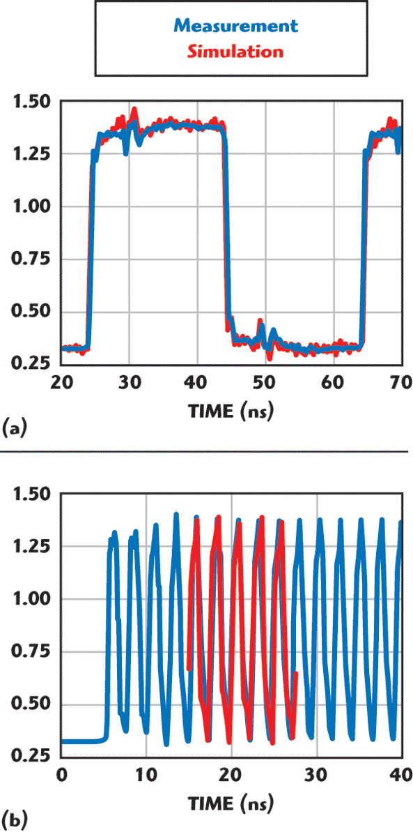
Simulated versus measured results for both 50 and 830 Mbps are presented in (Figure 7). Excellent agreement is observed.The full-channel simulation methodology is then employed to perform a number of design studies. A pseudo-random bit steam is introduced on the aggressor line and an eye diagram of the response is computed, as shown in (Figure 8). By examining the eye diagram crossovers, the maximum skew rate of the channel is determined.
Simulating Electronics in the Next Generation World
The ability to integrate EM-based S-parameter models, behavioral and transistor-level circuit models as well as digital models and effectively incorporate them into an existing design flow is illustrated by the design methodology adopted at Intel.
To maintain their leading position in the PC market, Intel has adopted a Design for Manufacturing (DFM) approach in which Design of Experiments (DOE) is used together with scripts, circuit and electromagnetic simulation tools to simulate and optimize over a wide range of computer operating conditions.
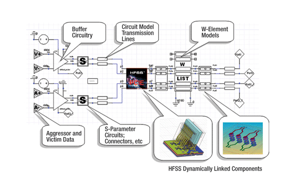
Previously, this approach incorporated simple models of electromagnetic effects and worked well in the design of earlier, slower speed computers. However, it proved inadequate at accurately predicting system behavior as slow parallel buses were being replaced by high speed serial buses including PCI Express and ATA. The block diagram of the new simulation requirements is presented in (Figure 9). In this figure, W-elements are used to characterize transmission lines, S-parameter models are adopted to characterize three-dimensional interconnects and planar electromagnetics solutions are used to characterize transitions.
A key feature of this methodology is the ability to perform rapid analysis and optimization on multiple levels of model accuracy. Initial design is performed at a high level using only behavioral and circuit level components. As the design is refined, circuit level models may be replaced by more detailed electromagnetic models using the unique Solver-on-Demand™ technology.
With this method, a one button click is all that is required to switch from a circuit level simulation to an electromagnetic level simulation. If the selected component has been previously solved using an EM solver, the model is cached and the pre-computed values are used; otherwise, the electromagnetic simulator is called and the precise electromagnetic solution computed. Since all parameters in geometry, materials and frequencies are common between the electromagnetic, circuit and system level simulators, it is easy to perform what-if analyses to optimize performance and ensure successful designs.
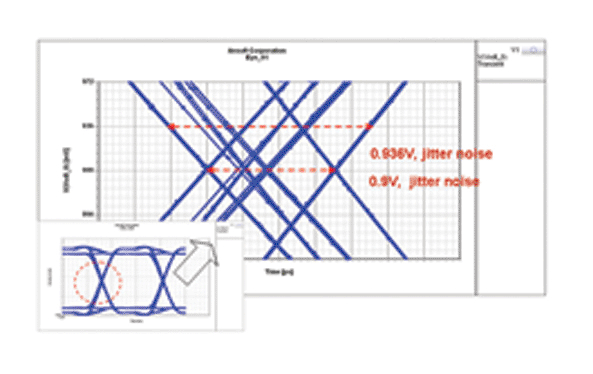
In addition, Intel requested a “by-pass” capability in the design management system that allows any component to be short circuited in the design. This allows designers to study the effect of each component individually as well as together on degrading signal propagation through the channel. (Figure 10) shows the eye diagram evaluated at a number of locations along the channel. By selectively by-passing each of these components, the amount of closure caused by each component can be evaluated and any signal degradation beyond specifications can be flagged. In the example shown, the connector had the largest effect on closing the eye.

Electromagnetics in the Environment
Along with understanding the interactions that occur between the chip, package and board levels, engineering teams often need to investigate the wider environment within which their devices operate. The proliferation of wireless devices has resulted in a setting where numerous devices are working in close proximity leading to potential signal interference. Mobile phones, GPS and RFID are just a few of the application areas where antennas are placed in close proximity to electronic circuitry; the actual and precise location of the antenna affects the system performance. As a result, antenna designers are increasingly performing simulations to characterize the interactions between the antenna and the electronics.
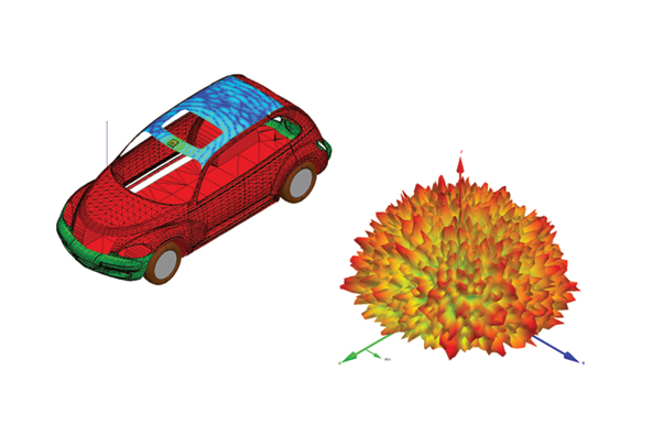
(Figure 11) shows the electromagnetic fields that result from a GPS antenna placed on the roof of a Chrysler PT Cruiser. To model these fields, the air space around the car was over 2500 cubic wavelengths. From these fields the radiation pattern of the antenna and car can be determined. Since the car body involves many large conducting surfaces, the resulting images produce a “sea urchin” radiation pattern.
Leveraging Today’s Compute Power
New compute architectures pack more processors into less space with large memory allowing massive simulations. While Intel and AMD are delivering multi-core processors with 64-bit architectures, system vendors like HP, Sun and others are working with multi-nationals to install ever more powerful compute farms.
Early on, Ansoft recognized this trend and developed 64-bit solvers, multithreaded architectures and new options like DSO (Distributed Solve Option). These new technologies allow designers to more rapidly explore device or system performance over a range of dimensions, orientations, material parameters and frequency. Sensitivity analysis, design of experiments, genetic algorithm optimizers, manufacturing tolerances and material variances are being combined to provide engineers with design insights that have never before been possible.
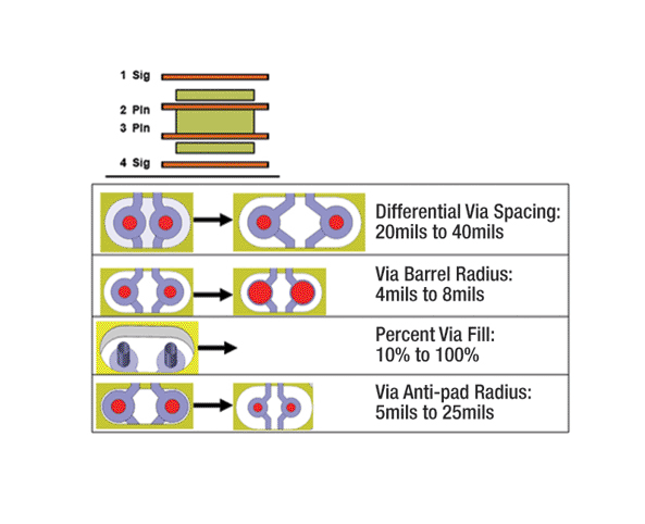
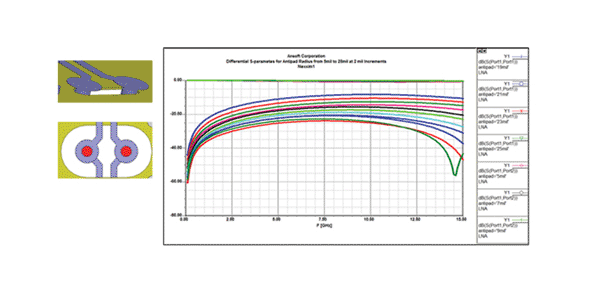
The power of these new methods can be seen using a simple example to study vias in a PCB. (Figure 12) illustrates a differential via structure with geometric parameters including spacing, barrel radius, percent fill and anti-pad radius. The goal is to minimize the return loss by adjusting these parameters. (Figure 13) shows a plot of the return loss and insertion loss performance as a function of anti-pad radius and the dramatic effect on return loss especially at the higher frequencies. Twenty-five CPUs, all managed from a single engineer’s desktop, were used for the simulations. The distributed network took only seven minutes to complete the simulations vs. 110 minutes using a single computer. In addition, data management software caches these solutions and makes them available to the circuit designer, so that upstream and/or downstream design changes can be made in concert with a variety of layout options for the vias.
Conclusion
Next generation electronics involves the convergence of RF, analog and digital devices into tightly coupled high performance systems. Design of these systems requires the integration of RF, analog and digital circuits with careful consideration of the new physics that occur with more closely spaced high performance designs. New solutions have been developed to combine 3D EM physics together with new algorithms for time and frequency domain circuit simulation. Special attention to integrate these new solutions into the existing design flows has been made and case studies that highlight the ability to include frequency dependant layout effects and simulate the larger, more complex circuits that result have been shown. In addition, new algorithms have been developed to leverage the power of new compute systems, providing designers with unprecedented insight prior to building prototypes.