Digital TV offers a far wider choice of TV viewing and a reduction of the interference that may be experienced on analog TV. Recently, many RF circuits realized in the CMOS process have been reported and the 0.18 mm process is a good candidate for highly integrated systems-on-chip (SOC) applications. The requirements of low power and low cost push the trend toward a single radio chip. Figure 1 shows the up-down architecture of a DTV RF tuner.1,2 The RF signal is upconverted to 1.2 GHz by the first mixer and then downconverted by the second mixer to the IF. Rather than bulky tunable filters used traditionally in direct-down architecture, the up-down architecture has the advantage of providing a good image rejection by using a 1.2 GHz bandpass filter.
For an RF TV tuner application, the LNA not only requires low noise and high gain but also high linearity and flat response over the 40 to 900 MHz frequency range. In this article, a broadband differential LNA with gain-control, using dual-feedback and shunt-shunt feedback topologies, is adopted to achieve high gain and a flat broadband response. The controllable gain can prevent saturation of the receiver when the input signal level is relatively high. The broadband LNA is implemented in a TSMC 0.18 mm CMOS process.

LNA Topology and Circuit Design
Figure 2 shows the block diagram of a DTV tuner differential RF front-end, in which the presented three-stage LNA includes two feedback amplification stages and one gain-control stage (see Figure 3). It uses dual-feedback and shunt-shunt feedback stages to achieve a high and flat broadband response. The dual-feedback stage is the first stage and the shunt-shunt feedback stage is the second stage, to increase the gain. The gain-control stage is used to prevent saturation.
It is known that the differential circuit can mitigate the effects of common mode noise. As shown, this LNA, which did not use a high impedance at the source terminal, is a pseudo-differential circuit structure. The reason not to use a true differential amplifier circuit is that, for low voltage RFIC design (1.8 V, for example) a high impedance at the source terminal will compress the voltage headroom and output voltage swing, which will reduce the amplifier gain. Also, this pseudo-differential LNA circuit can still reject the common mode noise from VDD.
Feedback Stages
The dual-feedback stage adopts the Kukeilka architecture.3–5 This architecture is a refinement of the traditional shunt-series feedback. The output of the dual-feedback stage is capacitively coupled to the shunt-shunt feedback stage input through a DC block capacitor.
The M1 and M2 of the dual-feedback stage dissipates 2 and 4 mA of DC current, respectively. The aspect ratios (W/L) of M1 and M2 are chosen to be the same. To ensure M1 is operating in the saturation region, the size of the diode-connected transistor, Mf1, is chosen to be twice that of M1. In addition, Cf1 is added in parallel with Mf1 to compensate the over-damped characteristic of this structure. However, the dual-feedback stage does not provide the desired gain for the LNA. In order to achieve a higher gain, a shunt-shunt feedback stage6 is added. M3 dissipates 6 mA of DC current and the shunt-shunt feedback stage dissipates 12 mA due to the differential topology.

Gain-control Stage
As shown, Mc1 is used to implement a gain-control mechanism. The voltage, Vctrl, applied to Mc1, controls the variable gain. This topology yields a negative slope gain-control curve. The LNA has its maximum gain when the control voltage is zero and vice versa.
Simulation and Measurement Results
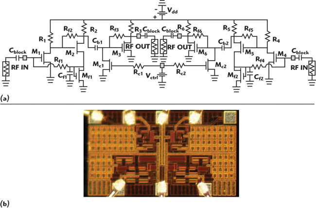
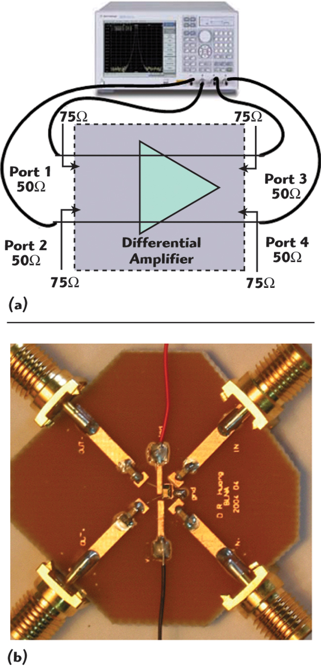
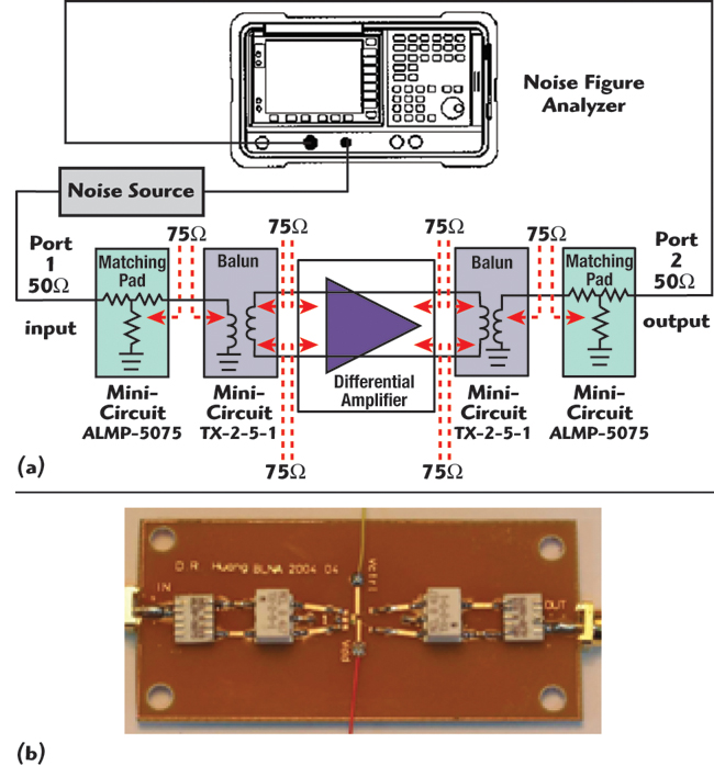
Figure 4 shows the complete circuit schematic and chip micrograph of the designed differential LNA. The chip die size is 1.007 × 0.568 mm. The circuit measurement is performed using an FR-4 PCB test fixture. For differential S-parameter measurements, a four-port network analyzer was used. Since the four-port analyzer can support differential measurement, no baluns are needed. Figure 5 shows the block diagram and photograph of the test fixture for differential measurement environment. It is noted that, although this circuit is designed for 75 Ω DTV systems, 50 Ω instruments are used for measurement. In order to match the two different characteristic impedances used in the system, matching pads (Mini-Circuit ALMP-5075) are used to convert the impedance from 50 to 75 Ω and vice versa. For single-ended instruments such as the signal generator, spectrum analyzer and noise figure analyzer, a balun (Mini-Circuit TX-2-5-1) is used to convert the differential input/output to single-ended input/output. Figure 6 shows the block diagram of the conversion scheme and a photograph of FR-4 PCB test fixture.
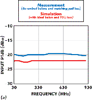
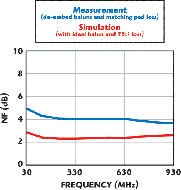
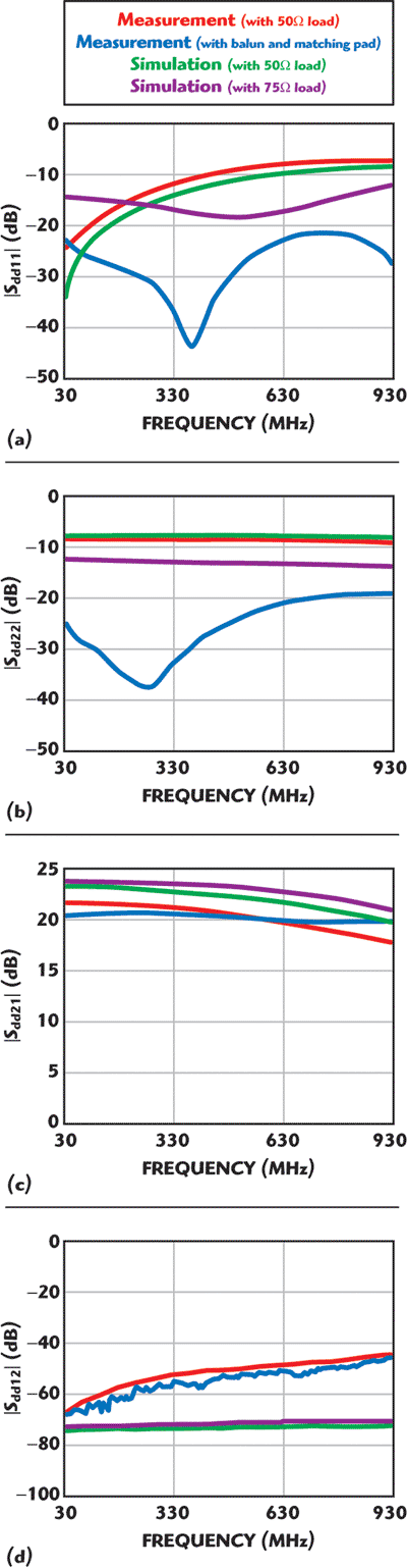
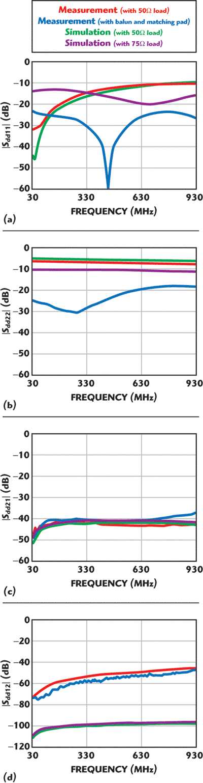
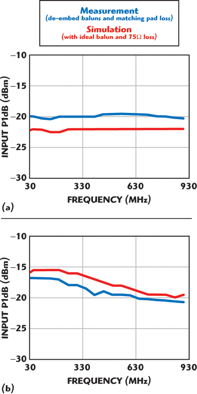
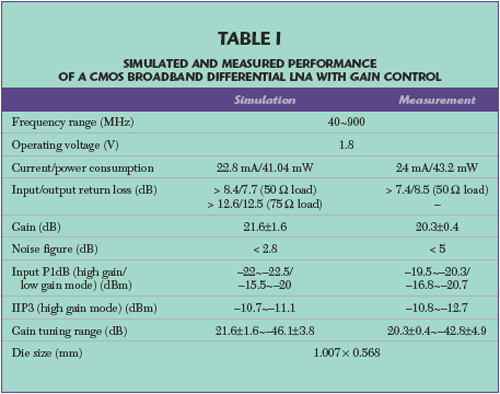
The simulated and measured results are shown in Figures 7 to 11, where the measurements of S21 and S12 are shown with the losses of the baluns and matching pads de-embedded. When the control voltage is zero (high gain mode), the LNA exhibits a gain of 20.26 ±0.41 dB, a noise figure less than 5 dB, an input P1dB between –19.5 and –20.3 dBm, and an IIP3 between –12.7 and –10.9 dBm from 40 to 900 MHz. When the control voltage is at 1.8 V (low gain mode), the LNA gain is –42.8 ±4.9 dB. The power consumption is 43 mW at VDD = 1.8 V. It is noted that for the S-parameters, since the measurement with 50 Ω systems and the simulation using 50 Ω loads show good agreement, it is believed that the measurements with a 75 Ω system (not provided) and the simulations will also be in good agreement. Table 1 gives a summary of the measured and simulated performance of the CMOS broadband differential LNA with gain control.
Conclusion
A 40 to 900 MHz CMOS broadband differential LNA with gain control, implemented in a 0.18 mm CMOS process, for a DTV RF tuner application is described. The LNA uses both a dual-feedback and shunt-shunt feedback topology to achieve a high and flat broadband response. The LNA is designed with 75 Ω differential input and output impedances. The chip die size is 1.007 × 0.568 mm. The circuit measurement is performed using an FR-4 PCB test fixture. Since typical measurement instruments are 50 Ω systems, matching pads are used in the measurement to match the impedances between 50 and 75 Ω. For single-ended measurements such as with spectrum and noise figure analyzers, a balun is used to convert the differential input/output to single-ended input/output. In the 40 to 900 MHz frequency range, the LNA exhibits a gain of 20.26 ±0.41 dB, a noise figure less than 5 dB, an input P1dB between –19.5 and –20.3 dBm, and an IIP3 between –12.7 and –10.9 dBm. The gain tuning range is from 20 to –42.8 ±4.9 dB over the 40 to 900 MHz range. The power consumption is 43 mW at VDD = 1.8 V.
Acknowledgment
The authors would like to thank the Chip Implementation Center (CIC) of the National Science Council, Taiwan, ROC, for providing the TSMC CMOS process.
References
- S. Birleson, et al., “Silicon Single-chip Television Tuner Technology,” 2000 ICCE Conference Digest of Technical Papers, pp. 38–39.
- B. Taddiken, et al., “Broadband Tuner on a Chip for Cable Modem, HDTV and Legacy Analog Standards,” 2000 IEEE RFIC Symposium Digest, pp. 17–20.
- C.D. Hull and G.B. Mayer, “Principle of Monolithic Wideband Feedback Amplifier Design,” International Journal of High Speed Electronics, Vol. 3, February 1992, pp. 53–93.
- F.T. Chien and Y.J. Chan, “Bandwidth Enhancement of Transimpedance Amplifier by Capacitive-peaking Design,” IEEE Journal of Solid-State Circuits, Vol. 34, August 1999, pp. 1167–1170.
- Y.C. Chen and S.S. Lu, “Analysis and Design of CMOS Broadband Amplifier with Dual-feedback Loops,” 2002 ASIA-PACIFIC Conference on ASICs.
- B. Razavi, Design of Analog CMOS Integrated Circuits, McGraw-Hill, New York, NY, 2001.
- B. Razavi, RF Microelectronics, Prentice Hall, Upper Saddle River, NJ, 1997.
- D.A. Johns and K. Martin, Analog Integrated Circuits Design, John Wiley & Sons Inc., Hoboken, NJ, 1997.
- D.E. Bockelman and W.R. Eisenstadt, “Combined Differential and Common-mode Scattering Parameters: Theory and Simulation,” IEEE Transactions on Microwave Theory and Techniques, Vol. 43, No. 7, July 1995, pp. 1530–1539.