In the past several years, the wireless local area network (WLAN) market has grown significantly due to the great demand for high speed wireless connectivity. Furthermore, there is a constant desire to keep power consumption, cost and size of the communication devices to a minimum. This has been possible thanks to continuing advances in integrated circuit (IC) technology allowing the development of devices capable of operating at multiple gigahertz carrier frequencies with data rates competitive with established wired alternatives.1,2 In 1999, the IEEE ratified two wireless networking communications standards named 802.11a and b. The 802.11b standard operates in the 2.4 GHz industrial-scientific-medical (ISM) band, using direct-sequence spread-spectrum (DSSS) modulation, while the 802.11a standard operates in the 5 GHz unlicensed national information infrastructure (UNII) band. On the other hand, 802.11a employs orthogonal frequency division multiplexing (OFDM) in order to compete more effectively with the peculiarities of indoor propagation.1 The UNII frequency band provides 300 MHz of spectrum at 5 GHz (see Figure 1). Those 300 MHz are divided into two frequency segments: a contiguous 200 MHz portion from 5.15 to 5.35 GHz and a separate 100 MHz segment from 5.725 to 5.825 GHz. Furthermore, depending on the allowed maximum level of transmitted powers, these frequency assignments are split into three equal domains. The bottom 100 MHz domain is limited to a maximum transmitted power of 50 mW, the next 100 MHz to 250 mW and the top 100 MHz to a maximum of 1 W (outdoor communications).3 OFDM modulation subdivides a carrier into several individually modulated orthogonal subcarriers, all of which are subsequently transmitted in parallel. This technique mitigates the effect of multi-path. In the 802.11a standard, each OFDM channel consists of 52 subcarriers in a 16.6 MHz bandwidth (channel spacing of 20 MHz); 48 subcarriers are for data, the rest are for error correction (pilot signals).2,3 Thanks to this subdivision, a variety of data rates with different modulations are possible, permitting different levels of service. Therefore, the data can be modulated with BPSK, QPSK, 16QAM, or 64QAM with data rates of 6 Mb/s, 12 Mb/s, 24 Mb/s and 54 Mb/s, respectively. The medium access control (MAC) protocol used to give multiple users access to a shared environment is the carrier sense multiple access with collision avoidance (CSMA/CA).3
The aim of this article is to implement a frequency synthesizer design flow. This design flow achieves two important improvements: prediction of the synthesizer specifications before its fabrication and reduction in the number of fabrication runs, minimizing the overall manufacturing cost and development time. The new generation systems that utilize OFDM modulation are extremely sensitive to phase noise, which is present in the up- and down-conversion synthesizers. Therefore, a proper prediction is essential to design a high performance device. A design flow has been implemented thanks to the development of a Matlab simulation tool that predicts the phase noise, spurious emissions and lock time of a frequency synthesizer with great accuracy before its fabrication. This procedure has been applied to the design of a frequency synthesizer for the IEEE 802.11a standard UNII band from 5.15 to 5.35 GHz. This synthesizer is part of a greater development, focused on the implementation of a heterodyne receiver built in a standard 0.18 µm CMOS technology. This choice is based on the continuing advances made in CMOS technology, which make high volume, low cost and high frequency solutions possible. Finally, since the 802.11a and HIPERLAN2 standards share many performance requirements for the RF signal processing blocks, this synthesizer will also be suitable for HIPERLAN2.1

Performance Requirements
A rigorous choice of the performance requirements for the synthesizer is fundamental in order to achieve a competitive device within the WLAN market. The most important performance requirements are the operating frequency, frequency stability, crystal reference frequency, phase noise, spurious emissions and lock time. The requirements have been obtained from the IEEE 802.11a and HIPERLAN2 standards, and considering the fact that in a system with OFDM multiplexing, the synthesizer phase noise introduces intercarrier interference (ICI) and leads to a degradation in the signal-to-noise ratio (SNR). The operating frequency of the synthesizer depends on the receiver architecture chosen, which is a heterodyne receiver with the second downconversion in quadrature, as shown in Figure 2. The main focus of this article is the implementation of the second local oscillator (LO2), which works at 3.2 GHz. An external 20 MHz crystal oscillator is used, matching up with the channel spacing for the IEEE 802.11a standard. Furthermore, this standard requires a maximum crystal frequency tolerance of ±20 ppm. Therefore, a crystal frequency tolerance less than that value is acceptable.3 OFDM systems exhibit a sensitivity to phase noise higher than single carrier modulations. Because of this, the phase-noise specification is a key point in the synthesizer design. For that reason, two phase-noise specifications have been considered: VCO phase noise at 1 MHz offset and synthesizer total integrated phase noise over the channel bandwidth (20 MHz). The phase-noise requirements at 1 MHz offset come from two considerations: interferer strength and sensitivity of the OFDM scheme to phase impairments. With respect of the first consideration, for the highest data rate of 54 Mb/s, the receiver sensitivity is –65 dBm, and allowing for an adjacent interferer 40 dB stronger than the desired channel, the VCO phase noise needs to be lower than –132 dBc/Hz at 17.3 MHz offset. This result has been obtained by integrating the phase noise over the adjacent channel (20 MHz) and assuming a pre-detection SNR of 19 dB for a BER of 10–6 in a 64-QAM system. Since the VCO phase-noise spectrum decreases 20 dB per decade, its value will be –107 dBc/Hz at 1 MHz offset. Furthermore, the degradation added by the second consideration must be included. The phase noise in the OFDM system introduces intercarrier interference (ICI) and leads to a degradation in SNR. For an SNR degradation less than 0.1 dB, the phase-noise specification at 1 MHz offset should be at least –110 dBc/Hz, assuming a 64QAM modulation with subcarrier spacing of 312.5 kHz and pre-detection SNR of 19 dB.4 Therefore, in order to meet the requirements for the IEEE 802.11a standard, the VCO should have a phase-noise performance of at least –110 dBc/Hz at 1 MHz offset.

What is left to be determined is the total integrated phase noise, which is related to the synthesizer bandwidth. The influence of this requirement in OFDM-WLAN systems is well explained by Côme, et al.5 According to this reference, a total integrated phase noise of –32 dBc results in low BER degradation for 64QAM modulation. Therefore, with the aim of fulfilling the requirements for the IEEE 802.11a standard, the total integrated phase noise must be at least –32 dBc. The spurious emissions also play an important role in the new generation of OFDM-WLAN systems. In an integer frequency synthesizer, the dominant spurious emissions appear at multiples of the reference frequency, matching up in this case with the crystal oscillator frequency. Using the first consideration made previously for the phase noise, the spurious emissions level should be at least –59 dBc.4Finally, the maximum setting time to switch from one channel to another is 1 ms.3
Accurate Prediction in Phase-locked Loops
Some aspects of the synthesizers, such as phase noise, spurious emissions and lock time (TL), can be key issues in a communications system design.6 As previously presented, the present-day systems that utilize OFDM modulation are extremely sensitive to phase noise. Additionally, the reference spurs have a notable influence on the adjacent channel interferer. A high performance design requires an accurate prediction of the phase noise, spurs and lock time. Therefore, a simulation tool has been developed using Matlab to solve this problem. This simulation tool analyses the influence of different synthesizer parameters, such as the output frequency (fout), reference frequency (fref), VCO gain (Kvco), charge pump current (Kf), loop bandwidth (ωp), spurs attenuation (ATTEN) and the division ratio (N), in the phase noise, spurs and lock time.7
Phase-locked Loop
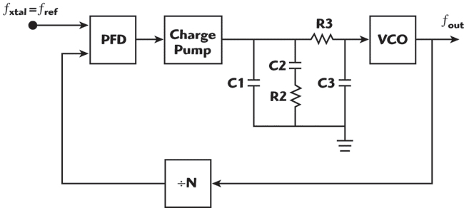
A phase-locked loop (PLL) is a feedback system that operates on the excess phase of nominally periodic signals. A PLL consists of a phase detector (PD), a low pass filter (LPF), a voltage-controlled oscillator (VCO) and two frequency divisors whose division ratios are N and R (see Figure 3). The filter impedance Z(s) is calculated as the ratio of the output voltage to the input current. The units of Kvco and Kf are Hz/V and A, respectively.
Spurs Level
The reference spurs, which appear at multiples of the reference frequency, can be classified into two kinds of spurious emissions: spurs based on leakage currents (leakage spurs) (Equation 1) and spurs based on charge pump mismatches (pulse spurs) (Equation 2)7

where base_leakage_spur is equal to 16 dBc and base_pulse_spur depends on charge pump mismatches, unequal transistor turn-on times and dead-zone elimination circuitry. Leakage is the parasitic leakage current through the charge pump, VCO and loop filter capacitors when the charge pump is in the tri-state state that is ideally high impedance. Finally, spur_gain can be calculated with Equation 3 and the total spur level is obtained by means of the sum of leakage_spurs and pulse_spurs

For older PLLs, where the leakage currents were in the microamp range, it is customary to model the reference spurs based entirely on leakage currents. However, modern PLLs typically have leakage currents of 1 nA or less, and therefore the pulse_spurs tend to be dominant, except at very low reference frequencies.
Phase Noise
The main PLL noise sources usually considered include: phase detector, VCO, crystal reference, frequency divider and loop filter. Equations 4 to 8 allow calculating the contribution to the total phase noise of each noise sources, respectively7

The normalized phase detector noise floor, L1Hz, is the phase detector noise floor when the reference frequency is 1 Hz and the filter noise, Lterm, is the thermal noise of any loop filter resistor. The transfer functions that multiply each noise source are obtained through the block diagram. The PLL total output phase noise can be calculated adding the contributions of each noise source given by Equations 4 to 8. At frequency offsets much lower than the loop bandwidth, the phase detector noise is dominant, although the crystal and divider noises can also be considerable. On the other hand, at frequency offsets greater than the loop bandwidth, the VCO phase noise is dominant. Depending on the VCO gain and the resistor values of the loop filter, the thermal noise will be comparable with the VCO noise.
Transient Response
The lock time that a PLL takes to switch from one channel to another is strongly dependent on the loop filter used. For example, the lock time to switch from frequency f1 to frequency f2, for a passive third-order loop filter, is given by Equation 107

Simulation Tool
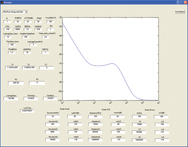
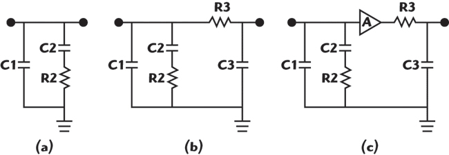
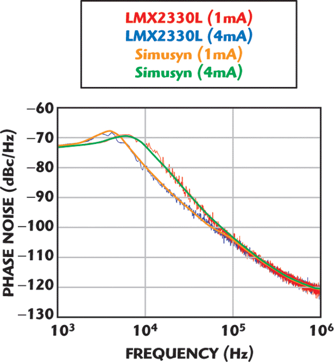
The phase noise, spurs and lock time prediction play a decisive role in the frequency synthesizers design. Furthermore, OFDM systems are highly sensitive to phase noise, which is present in the up- and down-conversion synthesizers. Consequently, a rigorous design requires an effective prediction to estimate accurately the phase noise, spurs and lock time. A simulation tool named Simusyn has been implemented using Matlab (see Figure 4). This software predicts the phase noise, spurs and lock time, and calculates the loop filter components for the following inputs: reference divider, crystal frequency, spurs attenuation, VCO gain, phase margin, L1Hz, loop bandwidth, output frequency, charge pump current, base_leakage_spur, base_pulse_spur, leakage current, frequency step and tolerance for lock time and divider, VCO and crystal reference phase noise. In addition, Simusyn allows using three kinds of loop filters: passive second-order, passive third-order and active third-order loop filters (see Figure 5). If the active loop filter is used, it is necessary to know the amplifier voltage gain (A) and its input noise voltage. The last step before starting the synthesizer design involves verifying the Simusyn results with the measured National Semiconductor’s LMX2330L commercial synthesizer. Phase noise, spurs and lock time have been verified for different synthesizer parameters. For example, in Figure 6, the phase noise for charge pump currents of 1 and 4 mA are presented. The rest of the basic parameters include: output frequency of 1.408 GHz, reference frequency of 1 MHz, spurs attenuation of 20 dB, loop bandwidth of 10 kHz and VCO gain of 60 MHz/V. The Simusyn software bases its results on the theoretical expressions shown in this section.7 Finally, the LMX2330L synthesizers have been controlled using Visual Basic software through the PC parallel port.
Determination and Prediction of the Synthesizer Specifications
It is essential to determine with great precision all the Simusyn inputs to achieve a high performance prediction. For that reason, the synthesizer architecture is chosen and the specifications of each block now must be deduced. Furthermore, this determination tries to be a rigorous design guide that can be used for other devices.
The proposed architecture is an integer-N frequency synthesizer with self-biasing current source and without a reference divider (see Figure 7). Furthermore, a passive third-order filter is employed to achieve additional filtering of the reference spurs. The frequency synthesizer consists of a phase-frequency detector (PFD), a high performance charge pump, an integer frequency divider and a VCO with self-biasing current source. The output signal of the VCO is divided by 160 and then is compared with a reference frequency of 20 MHz. Once the synthesizer architecture has been chosen, it is necessary to determine the general specifications of each block.
Voltage-controlled Oscillator
The voltage-controlled oscillator (VCO) is the core of the frequency synthesizer. A proper synthesizer design depends strongly on the VCO performance. The basic VCO specifications include: output frequency, frequency range, gain, output power and phase noise at 1 MHz offset. The output frequency has been established previously as 3.2 GHz.
The frequency range has been calculated considering the capacitive (four percent) and inductive (one percent) tank tolerances of the CMOS fabrication process with a safety margin of three percent. If the output frequencies were variable, the variation range would have to be included. The tank tolerances are obtained from the research team experience in the design of integrated inductors and varactors. The frequency range limits are fHIGH (3383 MHz) and fLOW (3031 MHz) and are given by Equations 11 and 12, where L, C and fosc are the inductor value, the varactor value and the VCO oscillation frequency, respectively


The VCO gain is deduced from the frequency range and tuning voltage. If the tuning voltage is varied from 0.5 to 2.8 V, since the mismatch of the sink and source currents of the charge pump is very high at the power supply rails, the VCO gain is 153 MHz/V.
The phase noise requirement was determined as –110 dBc/Hz at 1 MHz offset. Before designing the VCO, it is essential to verify that this requirement can be fulfilled. For this reason, the quality factor (Q) of the tank required to achieve the required phase noise has been estimated by means of Equation 13, which calculates the necessary quality factor to obtain a certain value of phase noise (+)8,9

Since the minimum differential input amplitude of the mixer employed in the frequency down-conversion is 0.5 V, a quality factor of 6.3 is necessary to obtain a phase noise of –110 dBc/Hz at 1 MHz offset, for a varactor capacitance of 0.8 pF and an excess noise factor of 2.13 This quality factor can be achieved using the inductors and varactors provided by the foundry libraries. For example, in these libraries, there are inductors with a quality factor of 10 at 3.2 GHz and varactors whose quality factor is greater than 40 at 3.2 GHz.10 Lastly, the output power depends on the mixer employed in the downconversion. In this case, the mixer is passive and needs a minimum input power of –3 dBm.
Charge Pump
The principal specification of this block is the charge pump current. Its value has been established to minimize the power consumption and taking into account that the capacitor in the loop filter next to the VCO is at least three times the VCO input capacitance.7 Thus, the charge pump current is set to 50 µA.
Loop Filter and Phase-frequency Detector
There are several specifications related to the filter design. First, it is necessary to choose the order of the loop filter and its gain (passive or active). It will be shown later that the VCO frequency range can be obtained with a passive filter, avoiding the amplifier noise. In addition, a third-order filter is selected to obtain an additional filtering of the reference spurs. There are two specifications related to the loop filter that are quite difficult to predict: L1Hz and base_pulse_spur.
The 1 Hz normalized phase detector noise floor has a considerable importance in the total integrated phase noise over the channel bandwidth. A priori, it is not possible to predict: L1Hz, but two methods have been used to estimate its value. The first is based on Equation 14, which calculates L1Hz according to the charge pump current, VGS–VT of the charge pump current source transistors, Boltzmann constant (K), temperature (T) and the time period during which the charge pump is active (tqp)8


This method is too optimistic, since using typical values of tqp (5 ns) and VGS–VT (0.5 V), L1Hz achieves the value of –216 dBc/Hz. Therefore, the second method will have to be applied. It involves utilizing the worst +1Hz of the bibliographic revision done by Banerjee7 about the 1 Hz normalized phase detector noise floor of different commercial synthesizers. Consequently, a 1 Hz normalized noise floor of –200 dBc/Hz is chosen. In addition, this value determines the loop bandwidth. By means of Simusyn and considering the VCO phase noise and the synthesizer total integrated phase-noise specifications, a loop bandwidth of 20 kHz is obtained. Finally, the base_pulse_spur is the last one to complete all Simusyn inputs. This specification is the most difficult to estimate because it depends principally on the charge pump mismatches, unequal transistor turn on times and dead-zone elimination circuitry. There are some expressions given,7 but they are not very useful in practice. The only solution entails selecting the worst base_pulse_spur (–292 dBc) of Banerjee’s bibliographic revision about the spur levels of different commercial synthesizers. In the following section, with the use of CADENCE, base_pulse_spur and +1Hz will be estimated with greater accuracy.
The values of the filter components are calculated using Simusyn by means of the well-known Application Note AN1001,15 with the following warnings: the phase margin must be chosen between 40° and 70°; the added spurs attenuation is chosen to fulfill the total spur requirements; and the capacitor in the loop filter next to the VCO is at least three times the VCO input capacitance. Therefore, using Simusyn, the values of the filter components are C1 = 701.88 pF, C2 = 3.06 nF, C3 = 70.18 pF, R2 = 4.39 kΩ and R3 = 340.13Ω for the following input parameters: crystal reference frequency of 20 MHz, ATTEN of 20 dB, a phase margin of 55°, a loop bandwidth of 20 kHz, an output frequency of 3.2 GHz, a charge pump current of 50 mA and a VCO gain of 153 MHz/V.
Furthermore, with the filter components previously calculated, the total reference spurs are at –73 dBc and the total phase noise of the synthesizer is shown in Figure 8, both results being obtained with Simusyn.

Synthesizer Building Blocks
Once the specifications of each block have been established, the design of each one is presented. Furthermore, the input specifications of the synthesizer will be determined with higher precision thanks to the use of CADENCE, allowing a more accurate prediction of its phase noise, reference spurs and lock time.
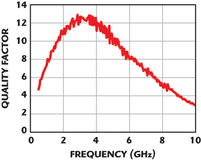
Figure 9 shows the schematic circuit of the VCO. The proposed architecture is a fully integrated differential NMOS VCO with a self-biasing current source. This architecture has been selected to maximize its tuning range. Two cross-coupled transistors with minimum dimensions M1 and M2 generate the negative impedance required to cancel the losses in the LC-tank. An oscillation safety factor of two and on-chip planar inductors have been used in this design. The key to the design of a low phase-noise oscillator is a high quality inductor. Therefore, a thick metal (2 mm) has been used to reduce the series resistance of the inductor. Its geometry has been selected to maximize the quality factor. As a result, two spiral inductors of 2.2 nH with a quality factor of 12 at 3.2 GHz have been employed. The electromagnetic simulation tool Momentum of ADS has been used to achieve high accuracy in its design. Before designing the VCO, the inductors have been measured and modeled. Figure 10 shows the measured quality factor of the inductor. As can be seen, this quality factor is optimized at the output frequency of the synthesizer (3.2 GHz).
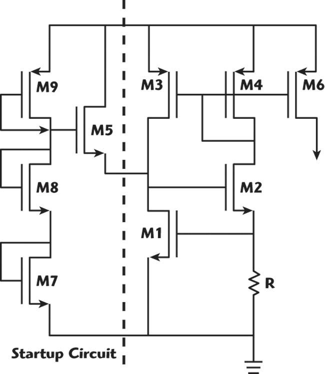
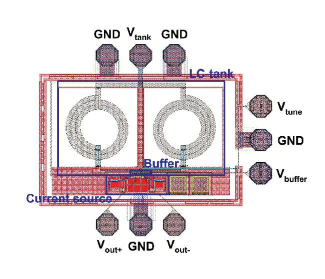
The varactors are P-N junction capacitors with a maximum capacitance of 0.88 pF. Each varactor is laid out with 65 fingers, which are 10 mm wide and 161 µm long. The quality factor of these varactors at 3.2 GHz is estimated to exceed 40. The varactors have also been previously measured. The current of the tank is supplied by the self-biasing source shown in Figure 11. A startup circuit has been employed to avoid Ibias being zero. The Ibias variation is lower than one percent for voltage supply variations of 10 percent.11 The layout of the VCO is shown in Figure 12, which measures 850 × 1000 mm2, including pads. The two inductors of the oscillator are situated at the top and the varactors are just below. The output buffer and negative resistance transistors are located in the middle of the die, whereas the current source is placed on the bottom.
Post-layout simulations allow determining the specifications of the VCO with high accuracy. In this way, the differential output amplitude of the VCO is 1.73 V, for a total tank current of 6 mA. This amplitude allows obtaining a phase noise of –120 dBc/Hz at 1 MHz offset. The phase noise and tuning range obtained from post-layout simulations are shown in Figures 13 and 14, respectively. In order to predict with Simusyn the phase noise, spurs and lock time with greater safety, the maximum VCO gain will be utilized (~250 MHz/V). This gain is reached when the tuning voltage is 2.8 V. Finally, in order to improve the VCO performance, the following layout issues must be considered: to ensure layout symmetry to minimize the even-order distortion in the differential output signal, the metal track in the tank must be as short as possible to reduce the parasitic capacitance and as wide as possible to reduce the parasitic resistance, choosing a compromise between both of them, differential pairs have a common center to minimize the effect of the process gradient, and to take into account the inductance introduced by the metal track that interconnects the two inductors.
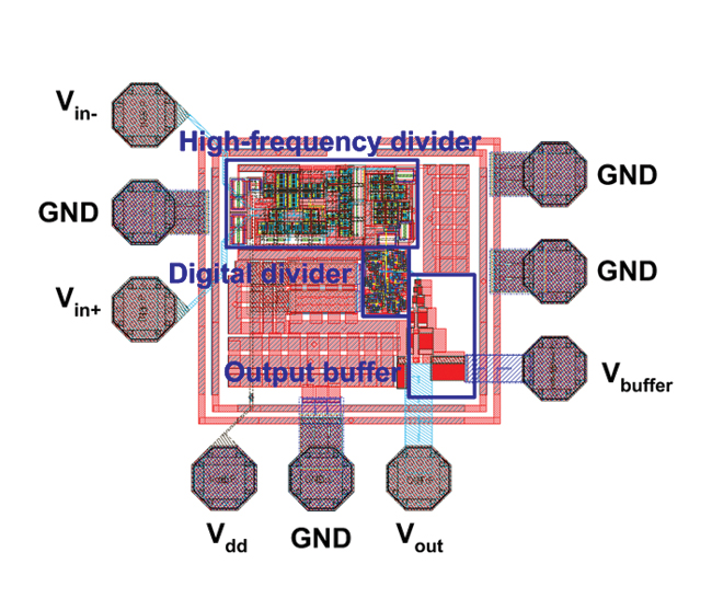
Frequency Divider
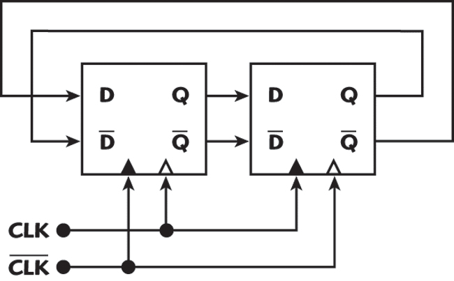
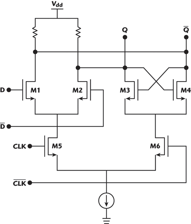
Figure 15 shows the divider block diagram. It consists of two high speed divide-by-2 and a digital divide-by-40. The block diagram employed to implement each high speed frequency divider is shown in Figure 16, which consists of two D flip-flops connected in a master/slave configuration. Each D flip-flop is triggered by two complimentary inputs clock signals, CLK and CLKBAR. Figure 17 shows the schematic circuit of a D flip-flop, which has been implemented using source-coupled logic (SCL).6 The main advantages of this architecture include: as it does not utilize PMOS transistors and the signal goes through only two gates per cycle, this topology is very fast; and it allows very small swings for the input clock. The digital divide-by-40 is made up of three divide-by-2 and one divide-by-5. These digital dividers are implemented with digital D flip-flops and Figure 18 shows their diagram.8 The design of the first two divide-by-2 has been done especially carefully due to the high specification frequency. Proper sizing of the transistors results in a reasonable speed-power trade-off at gigahertz rates. Since it is a differential device, the layout symmetry plays an essential role in its performance characteristics. The phase noise of the divider obtained from post-layout simulations is –143 dBc/Hz at 10 kHz offset. The layout of the divider is shown in Figure 19. It measures 663 × 734 mm2, including pads. The high frequency divide-by-4 is placed at the top and the digital divider is located just below. It has been necessary to include a buffer at the output of the divider in order to allow its measurement out of the synthesizer. This buffer is situated at the bottom of the layout. Lastly, the main layout issues, in order to improve the VCO performance, lie in the high frequency divider. As this divider is a differential circuit, the same differential recommendations proposed for the VCO can be also applied. Furthermore, the parasitic capacitances of this divider play an important role at high frequencies. With the aim of reduce them, the following issues must be taken into account: the most external metal layer must be used to make the interconnections, the parallel metal tracks must be very widely spaced, the length of all metal tracks must be minimized and crosses must be avoided between metal tracks.
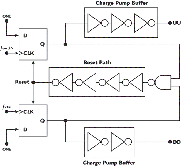
Phase-frequency Detector and Charge Pump
As shown in Figure 20, the phase detector employed is a phase-frequency detector (PFD), which consists of two digital D flip-flops, a logic gate NAND and a delay that is composed of a certain number of inverter gates. This delay in the PFD reset path is used to avoid the dead zone of the synthesizer, which is the region where the charge pump currents cannot flow proportionally to the phase error. In order to avoid the dead zone, the minimum reset delay of the PFD must be equal to the charge pump switching time. This time can be approximated by the average of the rise time and the fall time of the UU signal.13 The reset delay is also related to the reference spurs and L1Hz. For this design, four inverter gates have been employed. Figure 21 shows the schematic circuit of the charge pump.14 This architecture has been implemented to mitigate charge injection errors induced by the parasitic capacitors of the switches and current source transistors. A meticulous sizing of the charge pump transistors and a proper layout are essential for high performance since the reference spurs depend on the charge pump mismatches and unequal transistor turn-on times. The transistors M1 and M2 turn on at every phase comparison instant, therefore any mismatch between their magnitudes, duration, or absolute timing results in a net current that is drawn from the loop filter. Finally, the base_pulse_spur and L1Hz specifications must be predicted with high precision before building the device. They both have been specified by means of the CADENCE simulation tool. The normalized phase detector noise floor has been considered as a cyclostationary noise. A noise is cyclostationary if its autocorrelation is periodic in time. In this case, the origin is a periodic bias current generating shot noise. Therefore, Figure 22 shows the contribution of noise sources at 20 MHz to the total phase detector noise as a function of time. Calculating the average in a period, a phase detector noise of 2.7267 pA/Hz1/2 is obtained. From this result and by means of Equation 14, it is possible to calculate a 1 Hz normalised noise floor of –202.3 dBc/Hz. Consequently, a PLL noise floor of –85.2 dBc/Hz is achieved. Last of all, CADENCE must also be used to specify the base_pulse_spur constant with greater accuracy. Therefore, by processing the discrete Fourier transform (DFT) of the synthesizer output signal for different loop filters when the PLL is locked, a base_pulse_spur value of –289 dBc is obtained. Figure 23 shows the layout of the phase-frequency detector and the charge pump, which measures 850 * 1000 µm2, including pads. The PFD is situated in the middle and on the left, whereas the charge pump is located just on the right. A lot of effort has been put into the reduction of charge injections at the switching times. Coupling of the digital signals in the phase-frequency detector and the charge pump to the VCO through the power supply, and non-complete cancelling of the charge injection in the charge pump switches will modulate the output with a frequency equal to the reference frequency. The charge pump design has been optimised with respect to this aspect, and care has been taken to provide sufficient symmetry in the layout. The layout also contains some power supply decoupling capacitors.
Loop Filter
In the synthesizer architecture shown previously, an off-chip passive third-order filter has been employed to filter the charge pump pulses. As the VCO frequency range can be obtained with a tuning voltage variation from 0.5 to 2.8 V, a passive filter has been chosen. Furthermore, it is of a third-order to give an added attenuation to the reference spurs. Last of all, it is off-chip since the values of its components are too high to integrate them into the chip. Using Simusyn again and the application note AN1001,15 the values of the filter components are C1 = 1.14 nF, C2 = 5.01 nF, C3 = 114.7 pF, R2 = 2.68 kΩ and R3 = 208.16Ω. These values have been calculated utilizing the maximum VCO gain (˜250 MHz/V) in order to predict with Simusyn the phase noise, spurs and lock time with greater safety. This gain has been obtained by means of CADENCE and is reached when the tuning voltage is 2.8 V. The other Simusyn inputs to calculate these values coincide with those given in the determination and prediction of the synthesizer specifications section. Once all Simusyn inputs have been determined with high accuracy using CADENCE, it is possible to predict with Simusyn the phase noise and the spurs of the synthesizer minimizing the estimation error. Figure 24 shows the total phase noise of the synthesizer before its fabrication. In the same way, the reference spurs level obtained with Simusyn does not exceed –70 dBc. Both results fulfill the performance requirements.
Results
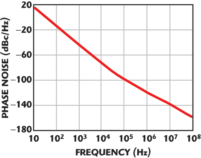
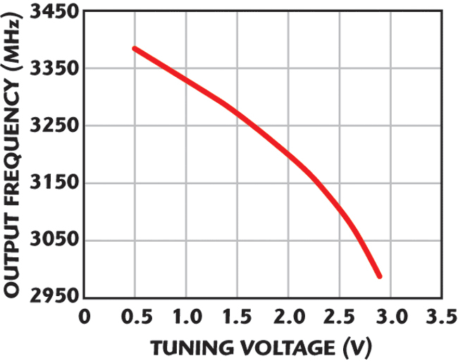
The WLAN synthesizer has been implemented using a 0.18 mm one-poly six-metal CMOS technology. Figure 25 shows a micrograph of the synthesizer die with an area of 1 × 1.2 mm, including pads. The circuit has been tested with a 3.3 V supply. The loop filter is not included on the chip because of the large values of its components. More than 300 MHz (11 percent of the center frequency) of VCO tuning range is achieved for a tuning voltage variation from 0.5 to 2.8 V. Figure 26 shows a comparison between the measured and simulated VCO tuning range. As can be seen, the operating frequency is reached when the tuning voltage is exactly half that of the power supply (1.65 V). The measured phase noise of the synthesizer is shown in Figure 27. This phase noise is compared with two phase-noise simulations. The blue simulation trace has been obtained with Simusyn for the inputs given, whereas the yellow simulation trace refers to the phase noise simulated with Simusyn when its inputs are specified with CADENCE. The phase noises at 1 and 17.3 MHz offset frequencies are measured to be –118 and –143 dBc/Hz, respectively, which agree well with the values of the last simulation. Therefore, the phase-noise measurements fulfill the initial requirements. The total integrated phase noise over the channel bandwidth does not exceed –32 dBc. Furthermore, the measured phase noise of the synthesizer at 17.3 MHz offset is shown in Figure 28. The phase noise of the synthesizer measured at offset frequencies beyond the PLL bandwidth is the inherent phase noise of the VCO. Thus, the phase noise of the VCO at 100 kHz offset is extrapolated to be –98 dBc/Hz, considering a slope of 20 dB per decade. As shown in Figure 29, the reference spurious tones are more than 64 dB below the carrier. This result is also much lower than the original requirement (–59 dBc). The power of the synthesizer differential output signal is approximately 0 dBm, which is much higher than the required power by the down-conversion mixer. Table 1 summarizes the performance of the synthesizer. Of the 53 mW total power consumption, less than 33.1 mW is consumed by the VCO. The self-biasing current source consumes 13.3 mW to supply a tank current of 6 mA. The frequency divider and phase detector consume 19.1 and 0.8 mW, respectively.
Finally, Table 2 presents some of the latest works reported on synthesizers, operating for IEEE 802.11a standard for the UNII band from 5.15 to 5.35 GHz. Clearly, the work in this article compares well with state-of-the-art designs in terms of phase noise, reference spurs, operation frequency and technology.
Conclusion
A low phase-noise fully integrated synthesizer, suitable for a 5 GHz wireless LAN receiver in the UNII band from 5.15 to 5.35 GHz, has been designed. Through the development of Simusyn, the synthesizer’s phase noise, reference spurs and lock time have been predicted with high accuracy before its fabrication. The use of high quality inductors, optimized at the operation frequency, allows obtaining a low phase-noise VCO. The use of a self-biasing current source in the tank provides a greater safety in the transconductance value and permits operation along more extreme operating points. The integrated synthesizer consists of a VCO with 0 dBm of output power and phase noise of –98 dBc/Hz at 100 kHz offset, a charge pump that mitigates the charge injection errors induced by the parasitic capacitors of the switches and current source transistors, and a fixed divide-by-160 circuit. The total phase noise of the synthesizer is –143 dBc/Hz at 17.3 MHz offset and the reference spurious does not exceed –64 dBc. With this phase noise and a loop bandwidth of 20 kHz, the total integrated phase noise of the synthesizer over the channel bandwidth is less than –32 dBc. Finally, the designed synthesizer consumes 53 mW with a power supply of 3.3 V.
References
- T.H. Lee, H. Samavati and H.R. Rategh, “5 GHz CMOS Wireless LANs,” IEEE Transactions on Microwave Theory and Techniques, Vol. 50, No. 1, January 2002, pp. 268–280.
- P. Zhang, T. Nguyen, C. Lam, D. Gambetta, T. Soorapanth, B. Cheng, S. Hart, I. Sever, T. Bourdi, A. Tham and B. Razavi, “A 5 GHz Direct-conversion CMOS Transceiver,” IEEE Journal of Solid-State Circuits, Vol. 38, No. 12, December 2003, pp. 2232–2237.
- “Wireless LAN Medium Access Control (MAC) and Physical Layer (PHY) Specifications: High Speed Physical Layer in the 5 GHz Band,” IEEE Standard 802.11a-1999, 2000.
- J. Bhattacharjee, D. Mukherjee, E. Gebara, S. Nuttinck and J. Laskar, “A 5.8 GHz Fully Integrated Low Power Low Phase Noise CMOS LC VCO for WLAN Applications,” 2002 IEEE MTT-S International Microwave Symposium Digest, Vol. 1, pp. 585–588.
- B. Côme, R. Ness, S. Donnay, L. Van der Perre, W. Eberle, P. Wambacq, M. Engels and I. Bolsens, “Impact of Front-end Non-idealities on Bit Error Rate Performances of WLAN-OFDM Transceivers,” Proceedings of the 2000 RAWCON, pp. 91–94.
- B. Razavi, RF Microelectronics, Prentice Hall, Los Angeles, CA, 1997.
- D. Banerjee, Performance, Simulation and Design, Second Edition, National Semiconductor, 2001.
- J. Craninckx and M. Steyaert, Wireless CMOS Frequency Synthesizer Design, Kluver Academic Publishers, Boston, MA, 1998.
- J. Craninckx and M.S.J. Steyaert, “A 1.8 GHz Low Phase-noise CMOS VCO Using Optimized Hollow Spiral Inductors,” IEEE Journal of Solid State Circuits, Vol. 32, No. 5, May 1997, pp. 736–744.
- http://www.umc.com.
- R.J. Baker, H.W. Li and D.E. Boyce, Circuit Design, Layout, and Simulation, IEEE Press, New York, NY, 1998.
- F.W. Grover, Inductance Calculations, Van Nostrand, New York, NY, 1962.
- H. Lee, T. Ahn, D. Jung and B. Park, “Scheme for No Dead Zone, Fast PFD Design,” Journal of the Korean Physical Society, Vol. 40, No. 4, April 2002,
pp. 543–545. - C. Lam and B. Razavi, “A 2.6 GHz/5.2 GHz Frequency Synthesizer in 0.4 mm CMOS Technology,” 1999 VLSI Circuits Symposium Digest of Technical Papers,
pp. 117–120. - W.O. Keese, “An Analysis and Performance Evaluation of a Passive Filter Design Technique for Charge Pump Phase-locked Loops,” National Semiconductor, Application Note 1001, May 1996.
- I. Vassiliou, K. Vavelidis, T. Georgantas, S. Plevridis, N. Haralabidis, G. Kamoulakos, C. Kapnistis, S. Kavadias, Y. Kokolakis, P. Merakos, J.C. Rudell, A. Yamanaka, S. Bouras and I. Bouras, “A Single-chip Digitally Calibrated 5.15 to 5.825 GHz, 0.18 mm CMOS Transceiver for 802.11a Wireless LAN,” IEEE Journal of Solid-State Circuits, Vol. 38, No. 12, December 2003,
 pp. 2221–2229.
 - A.R. Behzad, Z.M. Shi, S.B. Anand, L. Lin, K.A. Carter, M.S. Kappes, T. Lin, T. Nguyen, D. Yuan, S. Wu, V. Fong, A. Rofougaran and Y.C. Wong, “A 5 GHz Direct-conversion CMOS Transceiver Utilizing Automatic Frequency Control for the IEEE 802.11a Wireless LAN Standard,” IEEE Journal of Solid-State Circuits, Vol. 38, No. 12, December 2003, pp. 2209–2220.
- P. Zhang, L. Der, D. Guo, I. Server, T. Bourdi, C. Lam, A. Zolfaghari, J. Chen, D. Gambetta, B. Cheng, S. Gower, S. Hart, L. Huynh, T. Nguyen and B. Razavi, “A CMOS Direct-conversion Transceiver for IEEE 802.11a/b/g WLANs,” Proceedings of the 2004 IEEE Custom Integrated Circuits Conference, pp. 409–412.
- H. Rategh, H. Samavati and T. Lee, “A CMOS Frequency Synthesizer with an Injection-locked Frequency Divider for a 5 GHz Wireless LAN Receiver,” IEEE Journal of Solid-State Circuits, Vol. 35, No. 5, May 2000, pp. 780–787.
- F. Herzel, G. Fischer and H. Gustat, “An Integrated CMOS RF Synthesizer for 802.11a Wireless LAN,” IEEE Journal of Solid-State Circuits, Vol. 38, No. 10, October 2003, pp. 1767–1770.