There is an increasing demand for broadband multimedia components to satisfy the ever-increasing capacity of wireless networks. In particular, for dense local communications, the 60 GHz band for wireless personal area network (WPAN) applications is of special interest for short-range communications, due to the RF attenuation of the atmospheric oxygen by 10 to 15 dB/km, in a bandwidth of approximately 8 GHz, centered around 60 GHz. This makes the 60 GHz band of utmost interest for all kinds of short-range wireless communications.1 In order to pursue the RF system-on-chip (SoC) approach for a 60 GHz radio, antennas integrated with a low cost monolithically integrated CMOS RF front-end circuitry have been studied.2,3 In this article, a 60 GHz CMOS RFIC-on-chip dipole antenna is presented. A planar dipole-antenna structure with an integrated microstrip via-hole balun was adopted to design this RFIC-on-chip antenna. A FEM-based 3-D full-wave EM solver, Ansoft HFSS, is used for design simulation. The antenna chip is fabricated with a 0.18 μm CMOS process. On-wafer measurements of the input VSWR and the antenna gain of the designed RFIC-on-chip antenna were made with a microwave probe station.
Antenna Design
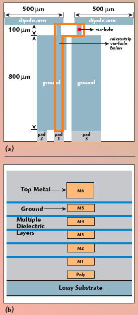
The proposed planar printed dipole antenna is shown in Figure 1. A microstrip via-hole balun acts as an unbalanced-to-balanced transformer between the feed coaxial line and the two printed dipole strips.4 The length of the dipole strips is approximately a 1/4 wavelength. The ground plane of the microstrip line and the dipole strips are in the same plane. As indicated, a via-hole permits the feed (point 2) of a printed dipole strip to have the same phase as the feed (point 1) of the other printed dipole strip. Due to the 180° phase difference between the top conductor and the ground plane of the microstrip line, the feed at point 2 of the printed dipole strip will have a 180° phase difference with the other feed at point 1. The widths of the dipole arm strips are chosen to be approximately one-tenth of a wavelength. The width of the microstrip feed-line is designed to have a characteristic impedance of 50 Ω. The accurate dimensions of each part of the printed dipole and integrated via-hole balun must be numerically computed to achieve the desired performance of the printed dipole antenna. Figure 2 shows the chip layout and the cross-section of the designed 60 GHz RFIC-on-chip dipole antenna fabricated with a 0.18 μm CMOS process.
Simulation and Measurement Results
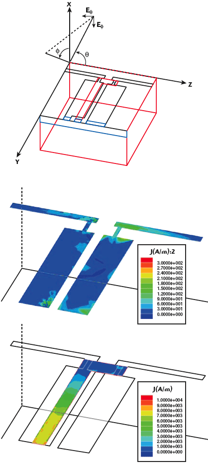
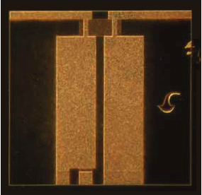
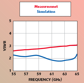
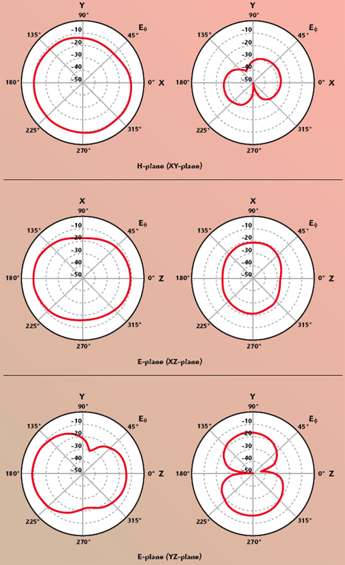
Figure 3 shows the HFSS simulated antenna current distribution. The simulated current density vectors on the top and bottom metals show the balanced current distribution and the 180° phase difference of the flowing current vectors at the two feed points of the printed dipole. This shows the working of the integrated microstrip balun. Figure 4 shows a chip micrograph of a fabricated 60 GHz CMOS RFIC-on-chip antenna. The chip size is 0.75 × 0.66 mm with a substrate thickness of approximately 500 mm. Figure 5 shows the input VSWR of the antenna, measured on-wafer, which is less than 3 from 55 to 65 GHz. Figure 6 and Table 1 show the simulated antenna radiation patterns and power gain values in the H- and E-planes at 60 GHz. Note that the antenna power gain (absolute gain), Gp, is defined as

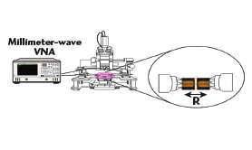
The simulated antenna radiation efficiency is approximately 16 percent, which may be due to the CMOS substrate loss. The H-plane pattern is close to an omni-directional pattern except for some attenuation in a certain direction. The simulated maximum, minimum and average power gains in the H-plane are approximately –9, –16 and –11 dBi, respectively. The absolute power gain of the antenna was measured on-wafer with the technique described by Simons and Lee.5 As illustrated in Figure 7, two identical RFIC-on-chip antennas are placed face-to-face within a distance R. One antenna is used as a transmitting antenna and the other as a receiving antenna. It is noted that the distance R separating the two identical antennas should satisfy the far-field condition, which is equal to or greater than5

where D and λ0 is the largest aperture dimension of the RFIC-on-chip antenna and the free-space wavelength at the operating frequency, respectively. From the Friis power transmission formula, the maximum antenna power gain (in the central forward direction of the dipole antenna) is given by

where
Gt and Gr = gains of the transmitting and receiving antennas
Pt = power transmitted
Pr = power received
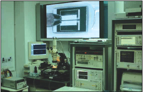
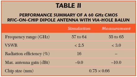
Similarly, since the two antennas are identical, Gr = Gt = G. The power ratio Pr/Pt is the measured direct transmission coefficient |S21|2 from the VNA. Figure 8 shows a photograph of the probe-station, on-wafer measurement setup. The measured maximum antenna power gain at 60 GHz is approximately –10 dBi, which is in good agreement with the simulation results. Table 2 shows the performance summary of the antenna radiation characteristics.
Conclusion

This article discussed the design, fabrication and on-wafer measurement of a 60 GHz millimeter-wave CMOS RFIC-on-chip dipole antenna with an integrated microstrip via-hole balun. This is to realize an RF system-on-chip (SoC) for a 60 GHz radio with the antenna integrated with a low cost, monolithically integrated, CMOS RF front-end circuitry. The antenna chip is fabricated with a 0.18 μm CMOS process with a chip size of 0.75 × 0.66 mm. The HFSS FEM-based 3-D full-wave EM solver is used for design simulation. The input VSWR and the maximum antenna power gain of the RFIC-on-chip antenna were measured on-wafer. The measured antenna VSWR is less than 3 from 55 to 65 GHz. The simulated H-plane radiation pattern is close to an omni-directional pattern and the simulated antenna radiation efficiency is approximately 16 percent, which may be due to the CMOS substrate loss. The measured maximum antenna power gain at 60 GHz is approximately –10 dBi, which is in good agreement with the simulation results. The integration of the designed 60 GHz RFIC-on-chip antenna with a 60 GHz CMOS RF front-end circuit will be pursued.
Acknowledgments
The authors would like to thank the Chip Implementation Center (CIC) of the National Science Council, Taiwan, ROC, for supporting the TSMC CMOS process.
References
1. Federal Communications Commission, Amendment of Parts 2, 15 and 97 of the Commission’s Rules to Permit Use of Radio Frequencies Above 40 GHz for New Radio Applications, FCC 95-499, ET Docket No. 94-124, RM-8308, December 15, 1995; available via: ftp//ftp.fcc.gov./pub/Bureaus/Engineering_Technology/Orders/1995/fcc95499.txt.
2. C.H. Doan, S. Emami, A.M. Niknejad and R.W. Brodersen, “Design of CMOS for 60 GHz Applications,” 2004 Proceedings of the IEEE Solid-State Circuits Conference, pp. 440–449.
3. Y.P. Zhang, M. Sun and L.H. Guo, “On-chip Antennas for 60 GHz Radios in Silicon Technology,” IEEE Transactions on Electron Devices, Vol. 52, No. 7, July 2005, pp. 1664–1668.
4. H.R. Chuang and L.C. Kuo, “3-D FDTD Design Analysis of a 2.4 GHz Polarization-diversity Printed Dipole Antenna with Integrated Balun and Polarization-switching Circuit for WLAN and Wireless Communication Applications,” IEEE Transactions on Microwave Theory and Techniques, Vol. 51, No. 2, February 2003, pp. 374–381.
5. R.N. Simons and R.Q. Lee, “On-wafer Characterization of Millimeter-wave Antennas for Wireless Application,” IEEE Transactions on Microwave Theory and Techniques, Vol. 47, No. 1, January 1999, pp. 92–96.