
The demand on mobile communications has grown over recent years. Today’s mobile communication systems use sophisticated signal processing to achieve high transmission rates. The challenges for the next generation wireless systems will increase even further, when designs will need to meet multi-standards and achieve reconfigurability. Evaluations of various integration strategies will need to be performed to verify the feasibility of the proposed integration approach, where issues such as performance, cost and risk need to be considered. The requirements of the varying communication standards differ over a very wide range in terms of center frequency, signal bandwidth, signal-to-noise ratio, linearity, etc. This will have an impact on all radio front-end building blocks, and require comprehensive trade-off analysis to select the best appropriate architecture and derive the individual circuit block requirements.
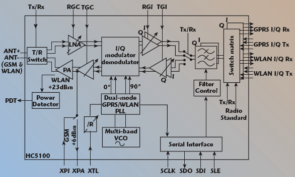
The complexity of digital signal processing is also steadily growing, as can be seen from the block diagram of a dual-band transceiver IC shown in Figure 1. The digital blocks offer the capability to compensate for some of the signal impairments caused by analog front-end blocks. To verify the complicated digital compensation algorithms, and the effect of analog nonidealities such as phase noise, nonlinearity and mismatch, the analog and digital blocks need to be simulated together. A key bottleneck to enable RF/baseband co-design is the presence of the RF carrier signal at several gigahertz in the RF front-end. To simulate the bit-error-rate (BER) or package-error-rate (PER) of a complete telecom link at the transistor-level and running thousands of cycles of the modulated signal is, at the very least, very expensive and often impractical.
Besides this performance verification, where the actual design is validated against specifications, another key requirement is the functional verification of the entire chip. Simple implementation errors at the interface between the digital control circuitry, which enable the various operating modes like power up, power down, receive, transmit and band selection, and the analog front-end, are often the cause of expensive reiterations. IC designers typically overcompensate and stick to budget requirements passed down from the system designer. The IC designer may be able to prove that a more relaxed specification within the IC will still meet system-level requirements. Yet, with no way to prove theory, time is spent optimizing circuitry that may not be necessary.
Systems involving baseband and analog/RF portions have traditionally been designed, simulated and verified separately due to the different mindsets of the engineers and the tools of the two domains. The goal during system-level design is to find an algorithm and architecture that implement the required functionality while providing adequate performance at minimum cost. During the actual implementation phase, however, RFIC designers also face several significant challenges. Considering a large IC, such as a wireless transceiver, high speed requirements make circuits extremely sensitive to parasitics, including parasitic inductance, passive modeling, as well as noise. Thus, the essence of the RFIC flow is the ability to manage, replicate and control post-layout simulations and effects, and effectively use this information at timely points throughout the design process. RFIC design also requires specialized and unique analysis techniques, which are specific to RF design. These techniques cross between frequency domain and time domain analysis methods, which are chosen on the basis of circuit type, designer comfort level, circuit size, or designer preference. Ultimately, this requires a seamless environment that facilitates the choice of simulation method. Integration trends have also affected the RFIC world, which used to be viewed as a separate, almost stand-alone entity. Today, many RFICs contain at least ADC, DAC and PLL functions, as well as a digital synthesizer, which is created through the digital environment and integrated on-chip. In some cases, an RF content is added to large SoCs as some design groups attempt a single-chip solution, while others are integrating by using system in package (SIP) techniques, which leads to similar verification issues as RFIC and SoC methodologies.
These challenges need to be addressed by a complete solution that must:
-
Provide comprehensive links between system-level design and IC implementation
-
Enable IC verification within a system-level context to leverage the existing wireless libraries, models and test benches
-
Allow full-chip mixed-level simulation at different abstraction levels (language neutral)
-
Allow for detailed analysis at the block and chip levels at an optimized simulation time
-
Manage and facilitate simulation with full parasitics
-
Contain layout automation that can be used at appropriate points in the design
-
Allow for several levels of passive modeling throughout the design process
All of the above requirements must be met through a single environment, which not only facilitates the job of the RFIC designer from the begining, but also integrates with the other domains such as analog/mixed-signal (AMS) and digital. This must include both a chip and block-level perspective at multiple abstraction levels, where the same design collateral can be passed back and forth, facilitating verification/implementation from either environment point of view, independent of the physical integration strategies.
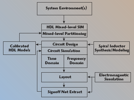
This article describes the Wireless RFIC reference flow as part of the RF Design Methodology Kit.1 The flow was developed and verified based on a realistic reference design. Therefore, the design of the dual-band transceiver IC was ported to a generic CMOS 180 nm process, with the subsequent use of the whole design database in workshops and at customer sites. Instead of coming from a tool feature angle, the flow definition started from the challenges and difficulties of the application-specific design issues described earlier. The Wireless RFIC flow is depicted in Figure 2. The flow is aimed at the RFIC designer and spans from the system design down to IC implementation, following the meet-in-the-middle approach described earlier.
Leveraging System-level Content
The design collateral from the system design process is used as the first, and highest, abstraction level. System-level descriptions become an executable test bench for the top-level chip. Models of the surrounding system can be combined with a high level model of the chip, producing an executable specification. System requirements serve as the first specification to drive the chip-level requirements and ultimately turn into repeatable test benches and regression simulations. Part of the leveraged system-level content is also the IP to determine the system relevant figures of merit, like EVM, BER and packet-error-rate (PER). Mixed-level simulation allows a natural sharing of information between the system and block designers. In order to enable the required links from the system environment to the IC environment, it is essential that the underlying multi-mode simulation solution is language neutral (from system models in C/C++, SystemC, SystemVerilog to digital/mixed-signal/analog behavioral HDL languages, down to Spice) and provides different engines and algorithms dedicated to the specific needs for a multi-domain circuit design.
Design Planning and Simulation
Successful execution on a complex design is contingent on the thoroughness of the planning up-front. No design can come together smoothly by accident. With a strong plan in the beginning that specifies top-level requirements, block-level requirements and the mixed-level strategies to use, a meet-in-the-middle approach can drive each block design to ensure full coverage of important design specifications and smoothly allow for blocks to have different schedule constraints. Therefore, the development of a comprehensive simulation strategy, which in turn leads to a modeling plan, is key.
After the realization of a first high level executable specification, the process continues by identifying particular areas of concern in the design. Plans are then developed for how each area of concern will be verified. The plans specify how the tests are performed, and which blocks are at the transistor level during the test. It is important to resist the temptation to specify and write models that are more complicated than necessary. Start with simple models and only model additional effects as needed. A formal planning process generally results in more efficient and more comprehensive verification, meaning that more flaws are caught early on, and there are fewer design iterations. The simulation and test plans are applied initially to the high level description of the system, where they can be quickly debugged. Once available, they can be applied during the mixed-level simulations of the blocks, reducing the chance that errors will be found late in the design cycle.
Multi-mode Simulation
The top-down process starts with HDL modeling for the entire RFIC added to the system-level test bench. This would include all RF blocks, along with any analog content and/or digital blocks. The first step is to behaviorally model the full chip within a top-level test bench, which would verify some system test such as EVM and BER. This at first verifies the partitioning, block functionality and ideal performance characteristics of the IC. This behavioral setup then serves as the basis to facilitate mixed-level simulations, where blocks can be inserted at transistor level and verified in a top-level context. This full chip and system setup can serve as the regression template to allow for continuous verification as blocks mature, allowing for a continuous evolution approach through the entire design. This is very important as any problems that are found can be detected at the earliest moment where time exists to fix the problem, and blocks can be designed in parallel to individual schedules.
Looking through the full simulation environment, several views of the same circuit will exist. This is likely to comprise a behavioral view, pre-layout transistor-level view and several views of parasitic information. As blocks mature, it may be required to add more transistor-level information to test RF/analog and RF/digital interfaces. This will require the use of a mixed-signal simulator capable of handling analog, digital and RF descriptions, and mix behavioral level with transistor-level abstractions. Picking the appropriate views of each block or sub-block, and managing the runtime versus accuracy tradeoffs, can be made through simulation options such as sending the transistors to a fast Spice simulator or keep the transistors in a full Spice mode. This configuration is highly dependent on the circuit and sensitivity of the interfaces. The ability to manage these configurations effectively is key, as they must be repeatable. This provides an effective mechanism to set up the continuous regressions that support the ACD.
Block Circuit Design
A preliminary circuit design then takes place, allowing for early circuit exploration and a first cut look at performance specifications. This early exploration leads to a top-level floor plan, which, for RFICs, is very sensitive to noise concerns and block-level interconnects.
At this stage, it is possible to synthesize passive components such as spiral inductors to specifications, and do their initial placement on the chip. This allows for two key activities: creating early models for spiral inductors that can be used in simulation before the block-level layouts are complete; and allowing for an initial analysis of mutual inductance between the spirals.
Component models of each inductor can be generated within this context for use in these simulations. Simulation is performed using the designer-preferred method, either in the frequency or time domain. This depends on the circuit, type of simulation, amount to be simulated and is a judgment call by the designer. A single process design kit and the associated environment allow for a smooth determination and selection of the simulation algorithm desired. The results are displayed through an appropriate display for the simulation type selected. As circuits are completed at block level, they are verified within the top-level context with behavioral stimulus and descriptions for the surrounding chip.
Physical Implementation
Layout automation (automated routing, connectivity driven layout, design rule driven layout, placement) can be used judiciously. The advantage to using layout automation is that it is tied to the schematic and DRC rules and allows for productivity gains. Analog capable routers can help with differential pairs and shielding wires, and allow for manual constraints per line. This allows for a physical design process that can also become repeatable just as the front-end process is. It may take some time and overhead to set up the initial tools, but this is made up as iterations are made through the design process. ECOs are more effectively performed if a repeatable layout process is in place. This is weighed against highly sensitive circuitry, which demands a manual approach.
Parasitic Extraction
As layouts are completed, electromagnetic simulation (EM) can be used to provide highly accurate models for passive components. For example, several spiral inductors may be selected as highly critical and are a target for EM simulation. These can be swapped in replacing the models that were created early in the design process, and mix and matched with the existing models. The designer then has full control over managing the spiral modeling process, again having the ability to trade off runtime versus accuracy at his/her choosing.
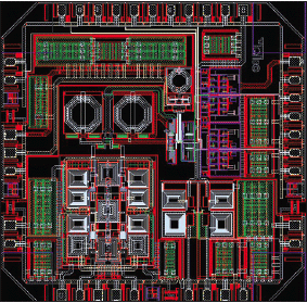
Net-based parasitic extraction becomes a key element of the process as layouts emerge. RF design is highly sensitive to parasitic effects. As such, the ability described above to manage different levels of parasitic information becomes paramount, as the designer can describe which areas, which lines and which blocks will have progressively more or less parasitic information associated with it. Less sensitive interconnects may require RC only, where more sensitive lines may require RLC. For lines with spirals attached, these can be extracted fully with RLC, plus the associated inductor component, even with substrate effects added for those lines that are the most sensitive, which are important to consider with respect to a compact layout (see Figure 3, which shows a large number of partially closely spaced spiral inductors). Again, these lines, which contain a ‘full’ extraction, can be mixed and matched with the component models for passive components that were created earlier.
Also, as the top-level layout emerges, analysis, especially substrate noise, is used to ensure that noisy circuits such as digital logic and perhaps PLLs are not affecting the highly sensitive RF circuits. The designer can check for this, and as areas of concern are flagged, either modify the floor plan accordingly or add guard bands around the noisy circuitry. However, it is often impractical to both simulate the entire design at the transistor level and include all the parasitic information. One approach is to extract calibrated behavioral models, using the extracted view of the design blocks. This, however, will not capture the effects of the parasitics on the interconnect between blocks. Therefore, hierarchical extraction capabilities to only extract parasitics of the interconnect between design blocks needs to be supported.
Calibrated HDL Models
Finally, as blocks are completed, the initial behavioral models can be back annotated for key circuit performance parameters, which can provide a more accurate HDL level simulation. While this will not account for every effect, it can add more realistic performance information at a very low runtime cost, allowing for faster level verification, and perhaps reduce the amount of full transistor-level verification required. In this way, the verification of a block by mixed-level simulation becomes a three-step process. First, the proposed block functionality is verified by including an idealized model of the block in system-level simulations. Then, the functionality of the block as implemented is verified by replacing the idealized model with the net list of the block. This also allows the effect of the block’s imperfections on the system performance to be observed. Finally, the net list of the block is replaced by an extracted model.
By comparing the results achieved from simulations that involved the net list and extracted models, the functionality and accuracy of the extracted model can be verified. From then on, mixed-level simulations of other blocks are made more representative by using the extracted model of the block just verified rather than the idealized model. When done properly, bottom-up verification allows the detailed verification of very large systems. The behavioral simulation runs quickly because the details of the implementation are discarded while keeping the details of the behavior. Because the details of the implementation are discarded, the detailed behavioral models generated in a bottom-up verification process are useful as blocks mature, or for third-party IP evaluation and reuse. Especially for wireless systems including RF front-ends, bottom-up verification is absolutely essential when verifying the performance of large systems. As mentioned earlier, RF-system simulations at the transistor-level running thousands of cycles of the modulated signal are often impractical. The use of advanced envelope analysis techniques instead of traditional transient simulation would only speed-up the process by a factor of 10 to 20 times. In addition, even bottom-up extraction using traditional passband models, where the RF carrier is still present, will not provide the required speed-up. Only the combination of bottom-up model extraction techniques in combination with so-called complex baseband or low pass equivalent models, where the carrier signal is suppressed, will lead to simulation times that enable package-error-rate analysis at full-chip level.
Generating behavioral models that include the detailed behavior of even simple blocks can be difficult and requires a specialized skill not commonly found in the design team. Therefore, automated tools and methodologies to generate detailed behavioral models with verified accuracy and an open application programming interface (API) to modify the existing templates according to specific application and/or technology needs are required.
Conclusion
Comprehensive trade-off analysis of the relevant figures of merit prior to and a continuous verification during the RFIC implementation is key for a successful design. The non-ideal effects that impact on the overall system performance need to be considered both during top-down modeling and within the bottom-up verification. Especially with the virtual prototype, crucial decisions regarding the architecture and block parameter specification could be made early on.

Jürgen Hartung
References
1. http://www.cadence.com/products/kits/RF_Design/index.aspx.
2. J. Hartung, I. Harasymiv, U. Erben, U. Klepser and S. Schneiders, “RF Architecture Selection Based on RF & System-level Test Bench Measurements,” Analog 2002 Konferenz, May 2002, Bremen, Germany.
3. R. Wittmann, J. Hartung, H.J. Wassener, G. Tränkle and M. Schröter, “RF Design Technology for Highly Integrated Communication Systems,” IEEE Computer Society DATE 03 Proceedings, March 2003, Munich, Germany, pp. 842–847.
Jürgen Hartung received his Dipl.-Ing. degree from the Technical University Darmstadt in 1993 and his Dr.-Ing. degree from Gerhard-Mercator University, Duisburg, in 1999. He joined Cadence in 1999 and has been project manager for various RF/analog/mixed-signal research activities. He is now technical marketing manager, focusing on the design flow for wireless applications. Prior to Cadence, he was a design engineer in the RF department of SICAN GmbH, Hanover, Germany.