
Frequency synthesizers have been well studied, but difficult problems sometimes arise in their practical implementations. The major concern of synthesizer designers is the phase noise. It is critically important in Doppler radar, frequency-agile radar and various communications systems. In such applications, a synthesizer’s phase noise may set the system’s limits for dynamic range and reception sensitivity. The choice of an optimal architecture for minimum phase noise, rejection of spurs from different sources, and achieving high efficiency and small volume are the key steps in an airborne synthesizer design. This article describes the design of a frequency synthesizer with the following performance:
-
The frequency varies from 8.9 to 9.3 GHz in steps of 20 MHz.
-
The phase noise is –80 dBc/Hz at 100 Hz and –97 dBc/Hz at 10 to 600 kHz frequency offset.
-
The synthesizer must use a 100 MHz reference with a phase noise of –115 dBc/Hz at 100 Hz.
-
The switching time is 20 μs to reach the frequency with an error less than 1 ppm.
-
The level of spurs is less than –64 dBc in the bandwidth from 10 MHz to the second harmonic of the output signal.
-
The level of the second harmonic is –48 dBc and the level of the third harmonic is –55 dBc.
-
The output power is +13 dBm and the power consumption is 2.3 W with a 12 V power supply.
-
The volume is 250 cm3 and the weight 470 grams.
Voltage-controlled Oscillator (VCO) Phase Noise Analysis: Choice of the VCO Band
A synthesizer consists of a voltage-controlled oscillator (VCO), a phase-locked loop (PLL) circuit and a reference signal source. The upper limit of a PLL IC frequency band is lower than the desired output frequency band, covering only half of it. There are two different ways to design a synthesizer—use a VCO at half the output frequency to produce the input signal to the PLL and then double it or use a VCO at the output frequency and then divide by 2 to produce the input signal to the PLL. The phase noise performance of the VCO is the main criterion to choose the best approach. The VCO phase noise is described by the Leeson equation

where
fOS = frequency offset (Hz)
F0 = oscillation frequency (Hz)
QL = loaded Q of the resonator circuit with an equivalent noise resistance R
fC = flicker corner frequency of the active device used as the amplifying element (Hz)
F = noise figure of the active device
k = Boltzmann’s constant, 1.38 10–21 (J/K)
T = temperature (Kelvin)
PS = average power of the signal at the input of active device (W)
K0 = oscillator voltage tuning gain (Hz/V)
The ![]() term describes the noise from the resistance R. It is usually significantly lower than the others and may be neglected.
term describes the noise from the resistance R. It is usually significantly lower than the others and may be neglected.
Then

where the noise floor NF describes the wide-band thermal noise in each side band, Pout is the oscillator output power in dBm, G is the gain of the active device in dB, f–3 = f0/(2QL) is the oscillator –3 dBm half-bandwidth.
Typical values of L(fOS) can be calculated for a published 4.3 GHz VCO1. This VCO has a 4 percent tuning bandwidth whose design is close to the one wanted for a synthesizer. The VCO consists of a series resonant circuit and a positive-feedback common-emitter amplifier using an AT-42086 silicon bipolar transistor from Agilent. The transistor noise figure is F = 8.5 dB. There is a significant degradation of the noise figure, because the input termination is far from optimal for minimum noise. The output power of the VCO is 10.5 dBm and the transistor gain is 8 dB. Then the NF = –167.8 dBc/Hz.
The total active resistance of the series resonant circuit is 12.8 Ω. The capacitive reactance of the series resonant circuit is 206 Ω and the loaded Q is 16.1, then f–3 = 130 MHz. An empirical value of 4 kHz for the flicker corner frequency has been determined for silicon bipolar transistors. For fOS = 100 kHz then, the calculated VCO phase noise is –105.5 dBc/Hz, while the measured phase noise is –104.4 dBc/Hz.
Typical values of L(fOS) can be predicted for a 9.1 GHz VCO based on the Leeson equation and compared with L(fOS) for a 4.55 GHz VCO (half of output frequency) with the same relative tuning bandwidth of 4.4 percent needed for the synthesizer. It is assumed that bipolar transistors are used in both VCOs, because they have a 10 to 15 dB lower phase noise than FETs.
The first degradation factor in a 9.1 GHz VCO is the increase of the output frequency. If f0 in the Leeson equation is multiplied to 2, then L(fOS) is increased by 6 dB in the fOS < f–3 region. Of course, this degradation is compensated by the frequency doubling of a 4.55 GHz VCO to produce the synthesizer output frequency.
The second degradation factor is that the transistor fMAX is higher for devices with smaller areas, and conversely, larger-area devices yield higher output power at lower frequencies. Therefore, Ps in Leeson’s equation for a 9.1 GHz VCO is typically 3 to 6 dB lower than that for a 4.55 GHz VCO. If the transistor noise figure remains constant for both VCOs, the noise floor of a 9.1 GHz VCO is typically 3 to 6 dB higher.
The third degradation factor is the decrease of QL, because the resonator’s capacitive reactance is divided by 2 when the frequency is doubled. Of course, the designer may use a smaller capacitance varactor to keep the capacitive reactance constant, but he may also use this varactor in a lower frequency VCO.
For example, a high Q microwave abrupt varactor GC1300 from Microsemi has a C(0V) = 1.2 pF, C(4V) = 0.8 pF. If it is series-connected with a 0.27 pF capacitor, it covers a 4.4 percent synthesizer bandwidth. The resonator capacitive reactance is equal to170 Ω at 4.55 GHz or 85 Ω at 9.1 GHz. If the total active resistance of the series resonant circuit remains constant for both VCOs, the loaded Q of the 9.1 GHz VCO is half and the phase noise is 6 dB higher than for the 4.55 GHz VCO. Since the phase noise of the 9.1 GHz VCO is 9 to 12 dB higher than for a 4.55 GHz VCO plus frequency doubler, a 4.55 GHz VCO is used in the synthesizer.
It is far more practical to consider VCOs or integrated oscillator subsystems as components and to purchase them from one of the specialized manufacturers. The HMC429LP4 integrated VCO from Hittite Microwave Corp. is the best choice for a 4.55 GHz VCO, because it has a 100 kHz offset SSB phase noise of –105 dBc/Hz and 4.4 to 4.7 GHz tuning bandwidth.

PLL Phase Noise Analysis: Choice of Optimal Architecture
The phase noise performance of a PLL is the main criteria to choose the best PLL architecture. The PLL noise model is shown in Figure 1. In this model, θref represents the reference phase and Δθref (s) represents the noise of the reference phase. The terms θin (s) and θout (s) represent the input and output phases of the PLL. 1/M and 1/N are the reference and main divider ratios. Kpd, F(s) and Kvco/s are the transfer functions of the phase detector, the low pass filter and the VCO. The term Δθpd (s) represents the PLL chip noise, including the noise of the dividers and phase detector. The RMS noise voltage of the filter (Ufn) is represented by the additional term Ufn (s). The noise of the VCO is represented by the term Δθvco (s). The open loop gain is given by

The transfer functions from the noise inputs to the PLL output are defined by
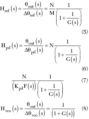
Usually, manufacturers give the phase noise data of the VCO, the reference source and the PLL chip as SSB phase noise Lvco(fos), Lref(fos) and Lpd(fos). The phase noise at the PLL output is given by

where

is the output phase noise from the VCO only,

is the output phase noise from the reference only,
is the output phase noise from the chip only,

is the phase noise from the filter only.

Integer-N PLL
The simplest PLL architecture is the integer-N PLL. In this case the output frequency is
fout = 2 FPD N
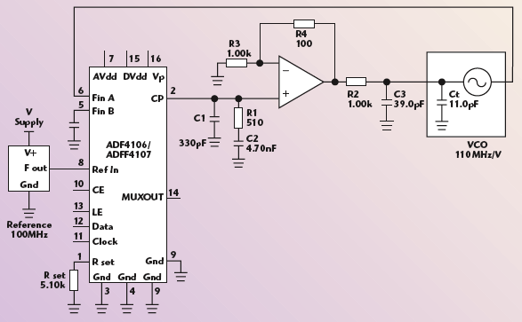
where FPD = 10 MHz is the frequency of the phase detector (half of the output step) and N = 445…465 is the main division ratio. An ADF4107 PLL chip from Analog Devices is used for the PLL, because it has a high input bandwidth (up to 7 GHz), a high phase detector frequency (up to 104 MHz) and low divider and phase detector phase noise (Lpd = –149 dBc/Hz at FPD = 10 MHz). A reference source MV87-1-100 MHz oven-controlled crystal oscillator (OCXO) from Morion Inc. is used for the PLL, because it has a low phase noise, –115 dBc/Hz at 100 Hz offset. A second-order passive charge pump filter2 is used for the PLL. The filter transfer function is its impedance. The frequency ωP of phase inflection point of G(s) is equal to the PLL bandwidth. At ωP, the phase term of G(s) has a maximum: φ(ωP) = –180° + φP. A common rule of thumb is to begin the PLL design with φP = 45°. However, it is recommended to slowly increase φP up to 53° with only a 1 dB overshoot at ωP in the Equations 5 to 8 transfer functions.
To achieve minimum phase noise at all offsets, the PLL bandwidth ωP must be set close to the point where the free-running VCO phase noise is equal to the overall PLL phase noise from other noise sources. If ωP is less, the PLL cannot improve the VCO phase noise at high frequency offsets. If ωP is more, the PLL begins to degrade the VCO phase noise at frequency offsets beyond ωP. From Equations 11 and 12, with φP = 53°, ω = ωP, N = 455, M = 10, Nref = –125.8 dBc/Hz and Npd = –94.8 dBc/Hz.
Assuming ω = ωP, the loop filter noise is much lower than Npd, and then Npd dominates over the other noise sources. From the VCO phase noise plot, fos = 75 kHz, at which Lvco is equal to –101 dBc/Hz. With ωP = 2π 75 kHz and calculating from Equation 9, Lout = –93.7 dBc/Hz. If φP and ωP are defined, the filter elements can be found: C1 = 1.66 nF, C2 = 13.1 nF, R1 = 483 Ω. To obtain the RMS noise voltage at the filter output, a practical resistor R1 can be substituted by an ideal resistor and an in-series connected equivalent noise source with a RMS voltage

The output phase noise from the filter only can be found from Equations 12 and 14,

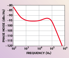
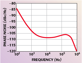
Calculations for fo = 75 kHz give Nfn = –112 dBc/Hz. To confirm the assumptions, the ADI SimPLL™ software from Analog Devices is used to simulate the PLL performance with the previously defined parameters. The open loop gain and phase plots are calculated with Equation 4 and shown in Figure 2. The output phase noise from the reference Nref (fos) only and the output phase noise from the chip Npd(fos) only are calculated from the manufacturer’s data with Equations 11 and 12 and shown in Figure 3. The output phase noise from the VCO Nvco(fos) only and the output phase noise from the loop filter Nfn(fos) only are calculated from the manufacturer’s data with Equations 10 and 15 and shown in Figure 4. The overall PLL output phase noise is calculated with Equation 9 and shown in Figure 5.
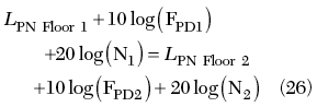
There are two regions in the PLL bandwidth. In the first region (fos < 500 Hz), the reference phase noise is the greatest of all noise sources. The synthesizer output phase noise (SPN) in the first region at fos = 100 Hz is given by

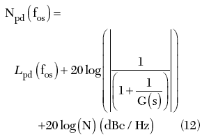
In the second region (1 kHz < fos < 50 kHz), the chip phase noise is the greatest of all noise sources. The chip phase noise dependence on the phase detector frequency is given by

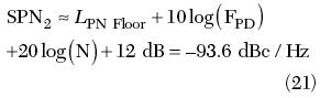
where LPN Floor = –219 dBc/Hz is the ADF4107 phase detector phase noise floor if FPD = 1 Hz. Therefore, in the second region, the synthesizer output phase noise is given by

Fractional-N PLL
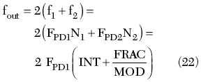
From Equations 16 and 18, it can be seen that to decrease SPN1 and SPN2, FPD must be increased and N must be decreased. However, N becomes fractional in this case. To operate with a fractional-N, a fractional-N PLL chip must be used. An ADF4193 chip from Analog Devices and a V630ME09 VCO from Z-Communications were used to simulate the performance of the fractional-N PLL. Because the maximum input frequency of the PLL chip is only 3.5 GHz, a multiplier by four is used to produce the synthesizer output signal. In this case, the output frequency is given by

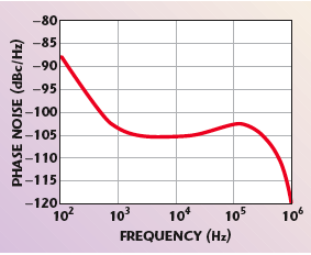
where INT is an integer part of N and FRAC/MOD is a fractional part of N. Because the maximum phase detector frequency of the ADF4193 is 26 MHz, FPD is set to 25 MHz (M = 4) and MOD = 25. Then, INT = 89…92, FRAC = 0…24 and a set of output frequencies with spacing of 4 FPD/MOD = 4 MHz is obtained. Only every fifth frequency of this set are used. The PLL phase noise versus frequency-offset plot is shown in Figure 6. The synthesizer output phase noise in the first region at fos = 100 Hz is given by

It is equal to the SPN1 at 100 Hz offset of the integer-N PLL, because the overall multipliers of the reference frequency in these synthesizers are equal. The synthesizer output phase noise in the second region is given by
There is a 4 dB improvement with respect to the integer-N PLL, because the FPD in a fractional-N PLL is also greater by 4 dB.
Hybrid Synthesizer
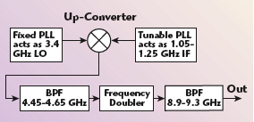
Another way to operate with fractional N is to use the hybrid synthesizer architecture with frequency translation,3 as shown in Figure 7. This architecture contains the first fixed integer-N PLL with maximum available FPD and the second tunable integer-N PLL. The signals of these sources are combined in the mixer, filtered and doubled. The output frequency is given by
where the terms f1 and f2 are the frequencies of the first and second PLL. The phase detector frequency of the fixed PLL FPD1 is 100 MHz to operate with the maximum available FPD. The phase detector frequency of the tunable PLL FPD2 is half the output step or 10 MHz.
Equation 22 represents the “virtual” fractional-N PLL with FPD = 100 MHz. The coefficients in Equation 22 are

where int(x) is the operation of taking only the integer part of the variable x.
The chip phase noises of the first and second PLLs are independent, because they are generated by two independent chips. Therefore, if they are equal, their combination has a minimum
An ADF4107 is used in both PLL, because it has a minimum PN floor. Therefore
10 log(FPD1/FPD2) = 20 log(N2/N1)
then N2/N1 = 3.16
In order to produce fout and to keep the minimum input frequency of the ADF4107 (1.0 GHz), N1 = 34, N2 = 105…125 can be obtained. Then, from Equations 24 and 25,
INT = 34 + 10…12 = 44…46,
FRAC = 0…9
Therefore, the values of the PLL frequencies are f1 = 3400 MHz, and f2 = 1050…1250 MHz.

The HMC389LP4 VCO from Hittite Microwave Corp. is used to simulate the performance of the fixed PLL. The phase noise versus frequency offset plots for the first and second PLLs are given in Figures 8 and 9.
The levels of the chip’s phase noise are approximately equal to –107 dBc/Hz. Their combination at 4.45 to 4.65 GHz has a phase noise 3 dB greater, because they are independent: –104 dBc/Hz. SPN2 is equal to –104 + 6 = –98 dBc/Hz. There is an 8 dB improvement with respect to the integer-N PLL, because FPD in the hybrid synthesizer is greater than 10 dB, but the degradation from the combination is only 3 dB. At a 100 Hz offset, the phase noise of both PLLs and the combined phase noise are calculated from
L1 ª Lref + 20 log(N1/M1) =
–115 + 30.6 = –84.4 dBc/Hz,
L2 ª Lref + 20 log(N2/M2) =
–115 + 21.2 = –93.8 dBc/Hz
LΣ = 20 log(antilog(L1/20) + antilog(L2/20)) = – 81.9 dBc/Hz
SPN1 is equal to –81.9 + 6 = –75.9 dBc/Hz. It is equal to the SPN1 of the integer-N PLL, because the overall multipliers of the reference frequency in these synthesizers are equal. It can be seen that any architecture cannot improve the reference phase noise, but a hybrid architecture improves the chip phase noise by up to 8 dB.
Practical Frequency Translation Architecture
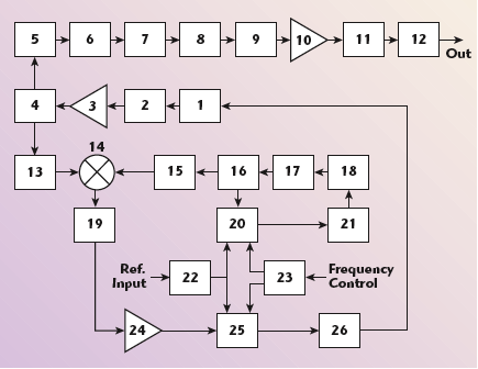
There are two disadvantages in the frequency translation architecture—the low level of the mixer output and the high relative level of mixer spurs. A modified practical architecture is shown in Figure 10. The HMC429LP4 VCO (1) generates a 4.45 to 4.65 GHz signal. After an isolator (2) and an FET amplifier (3) the signal, with a +14 dBm power level, is divided by a power divider (4) into two parts. The first part goes to the FET frequency doubler (6) through an isolator (5). The second part goes to the HMC213MS8 double-balanced mixer (14) from Hittite Microwave through an isolator (13) and acts as the LO.
The fixed 3.4 GHz PLL contains an HMC389LP4 VCO (18), an isolator (17), a power divider (16), an ADF4107 PLL chip (20) and a passive three-pole loop filter (21). The 3.4 GHz signal from the power divider (16) goes through a harmonic filter (15) to the RF input of the mixer (14) with a power level of –10 dBm. The mixer (14) translates the 4.45 to 4.65 GHz LO frequency to the 1.05 to 1.25 GHz IF frequency. Then the IF signal goes through a low pass filter (19) and an MMIC amplifier (24) to the ADF4107 PLL chip (25) with a power level of +2 dBm. The tuned 1.05 to1.25 GHz PLL contains a chip (25), an active three poles loop filter (26) and becomes a “virtual VCO” with sensitivity and phase noise similar to the HMC429LP4 VCO. After the frequency doubler (6), the signal goes through the isolator (7) to the bandpass filter (BPF) (8). The signal then goes through the isolator (9) to the two-stage FET amplifier (10). After amplification, the +16 dBm signal goes through an isolator (11) and a harmonic filter (12) to the output, where it emerges with a +13 dBm level. The reference signal from the external 100 MHz OCXO is amplified by the amplifier (22) and goes to the PLL chips (20, 25). The frequency control TTL signals go to the ADuC814 Micro-Converter (23) from Analog Devices. It writes the control bits into the PLL chips.
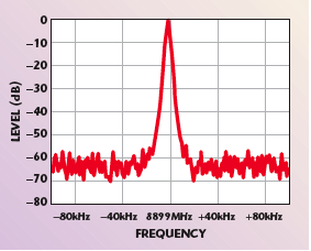
There are two differences between this architecture and the previous one. First, the 4.45 to 4.65 GHz signal is generated by the VCO at a higher power level and acts as the LO of the mixer. Second, the mixer acts as a down-converter and operates at lower power levels for both 3.4 and 1.05 to 1.25 GHz signals. As a result, a higher power level for the desired signal and a lower level for unwanted signals are achieved at the doubler’s input. This is very important, because the frequency doubler can produce high order spurs, which can arise within the bandwidth of the BPF (8). The output spectrum of the synthesizer, measured with a HP8592A spectrum analyzer with a resolution bandwidth of 3 kHz, is shown in Figure 11. A 6 dB attenuator is connected to the synthesizer output. The measured average noise level at 20 to 100 kHz offset frequencies is approximately – 63 dBc. Then, the average noise level in dBc/Hz is given by
Lout (dBc/Hz) = Lmeasured (dBc) – 10 log (3000) = –97 dBc/Hz
which agrees well with the theoretical result of –98 dBc/Hz.
Rejection of Spurs in Practical Architecture
There are three sources of spurs in the practical architecture - the mixer, the frequency doubler and the PLL charge pumps. The mixer (14) has a –33 dBm, 3.4 GHz, RF leakage at the LO input. The isolator (13) attenuates this signal down to –50 dBm. The frequency doubler produces high order spurs over a wide bandwidth, but the spur at the unwanted 3.4 GHz has a very low power level. The desired signal at the doubler output is the second harmonic and all other harmonics are unwanted and must be rejected by the BPF (8). The synthesizer’s output level for the 4.5 GHz spur is –64 dBc. The BPF (8) has a rejection level for the third harmonic of approximately 48 dB, with an extra rejection of 20 dB provided by the filter (12). The PLL charge pump spurs are the result of the charge pump unbalance and the DC current at its output. The total leakage current IL on the charge pump output can be assumed to combine all sources of leakage. The charge pump current waveform I(t) is a periodic series of short pulses with an Icp amplitude and an FPD repetition frequency. The relative level of the first spurs can be found from the Fourier transform of this signal and FM theory as

where Z1 is the loop filter impedance2 at the frequency FPD.
First, the maximum spur level is calculated for a fixed 3.4 GHz PLL. The PLL parameters are: FPD = 100 MHz, Kvco = 2π·50 MHz/V, Kpd = 5 mA/(2π rad), N = 34, φP = 53°, ωP = 2π 300 kHz. The loop filter elements are: C1 = 692 pF, C2 = 5.49 nF, R1 = 289 Ω. The loop filter impedance is Z1 = 2.3 Ω. The leakage current at the tuning port of the VCO (18) is 10 μA maximum. Equation 27 gives the value of the maximum spur level: L1 = –99 dBc. It is an acceptable value, but an extra RC LPF with a 3.0 MHz pole frequency is added to reject a 100 MHz EMI from the reference source. This additional RC circuit forms a third-order passive loop filter, which is placed as closely as possible to the tuning pin of the VCO (18). It produces an additional 30 dB attenuation of the reference frequency. The synthesizer’s output first spur level is –123 dBc and cannot be measured.
In the tunable 1.05 to 1.25 GHz PLL, the leakage current at the tuning port of the VCO (1) is 10 μA also, but the phase detector frequency is 10 MHz. The same loop filter as filter (21) rejects this spurs only to –51 dBc (first output spur). An active third-order 350 kHz loop filter with a 3.2 MHz last pole is used to reject the charge pump spurs. Its schematic is shown in Figure 12. The operational amplifier (op-amp) is a low noise OP184FS from Analog Devices. The main advantage of the active filter is the reducing of the leakage current down to 0.6 μA. It decreases the level of the first output spurs to –72 dBc. Their measured level is –70 dBc.
Rejection of Spurs from the Power Supply Unit
Achieving high efficiency is very important for airborne equipment. All the components of the synthesizer require a power supply voltage of +3.0 or +5.0 V, but the power supply voltage available is +12 V. A DC-to-DC step-down converter solves this problem, but it becomes the fourth source of spurs and extra phase noise in a common small-volume housing of 190 cm3. High grade rejection of electrical and magnetic noises from the DC-to-DC converter is needed.4,5 There are two paths through which these noises propagate—conductive and through the magnetic field of the converters inductors. This last path is rejected by using self-shielding inductor cores with small air gaps. The conductive path has two modes of propagation—common-mode and differential-mode. The common-mode is rejected by suspending the converters PCBs in the housing (decreasing the parasitic capacitance to ground) and using common-mode chokes at the input and output of the converters. The differential-mode ripple and noise are rejected by LC-LPF and voltage regulators ADP3301 from Analog Devices. The PLL does not work at the 260 kHz converter’s switching frequency and the VCO (1) is approximately in a free-running condition. One finds 260 kHz spurs from the ripple of the power supply. The level of sinusoidal FM spurs at the output of the VCO is given by4,5

where
Um = peak modulation voltage
Fmod = 260 kHz
Kp = 2π14 MHz/V is the pushing sensitivity
The DC-to-DC converter has 20 mV peak output ripples, the LC-LPF ripple rejection is 34 dB and the ADP3301 ripple rejection is 35 dB. Then, Um = 7 μV, LVCO(1) = –74 dBc and the synthesizer’s output spurs are 6 dB higher: –68 dBc.
The ripples go to the tuning port of VCO through the charge pump supply line. The charge pump has a power supply rejection ratio (PSRR) probably greater than 20 dB, but the tuning sensitivity Kvco = 2π110 MHz/V is 18 dB greater than the pushing. Therefore, the output level of the 260 kHz spurs from ripple on the tuning port is less than –70 dBc. Another path to the tuning port of the VCO (1) is the supply line of the operational amplifier (26). However, the PSRR of the OP184 is approximately 30 dB in the 100 to 300 kHz band. Therefore, the output spur level from this path is –80 dBc. Combining these spurs results in output spur levels of –63 dBc. The measured level of the converter spurs at the synthesizer’s output is approximately –65 dBc.
Wideband Noise in the Practical Architecture
To design an optimal PLL, its bandwidth must be set closely to the point where the free-running VCO phase noise is equal to the chip phase noise. However, in practice, the noise of the power supply and of the loop filter elements must be taken into account. The phase noise at 200 kHz offset frequency must be found from the voltage noise on the supply line of VCO (1) under free-running conditions. The phase noise level at the output of the VCO is given by4,5

The ADP3301 voltage regulator has an output noise voltage density UNS = 40 nV/![]() at fos = 200 kHz. Then, the supply PN is equal to –114 dBc/Hz. The total noise voltage density at 200 kHz, Ufn, at the tuning port of the VCO (1), must be found. There are seven independent sources of this noise—the noises of resistances R1 to R4 and the op-amp equivalent input noise voltage and current. The seventh is the noise of the voltage regulator, which goes through the charge pump with a minimum of 20 dB attenuation and through the op-amp with a 30 dB attenuation.
at fos = 200 kHz. Then, the supply PN is equal to –114 dBc/Hz. The total noise voltage density at 200 kHz, Ufn, at the tuning port of the VCO (1), must be found. There are seven independent sources of this noise—the noises of resistances R1 to R4 and the op-amp equivalent input noise voltage and current. The seventh is the noise of the voltage regulator, which goes through the charge pump with a minimum of 20 dB attenuation and through the op-amp with a 30 dB attenuation.
After RMS combining, the total noise voltage density at 200 kHz at the tuning port of the VCO (1) can be found: Ufn = 7.8 nV/![]() . The VCO output phase noise can obtained from Equation 29
. The VCO output phase noise can obtained from Equation 29
PN tune = 20 log(KvcoUfn /(![]() 2πfos)) = –110.3 dBc/Hz
2πfos)) = –110.3 dBc/Hz
The VCO (1), with a “clean” power supply and a “clean” tuning voltage, has an Lvco = –111 dBc/Hz at 200 kHz offset. Therefore, the total phase noise of VCO (1) at 200 kHz offset, in a practical architecture, is
Lvco(1) = 10 log(antilog(Lvco/10)
+ antilog(PN supply/10)
+ antilog(PN tune/10)) =
–106.7 dBc/Hz
The chip phase noise is equal to –107 dBc/Hz. If the PLL bandwidth is set at 200 kHz, then a 3 dB overshoot is generated at the 200 kHz offset frequency. Thus, the PLL bandwidth is set at 350 kHz and φP at 60°.

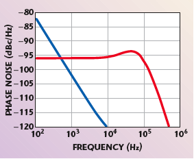
The measured output spectrum of the synthesizer, measured with a 10 kHz resolution bandwidth over a 2 MHz span, is shown in Figure 13. There is extra phase noise in the 300 to 1000 kHz offset frequency range, compared with simulation results. From Equation 1, it can be seen that the phase noise response must have a slope of –20 dB/decade above 350 kHz. However, the figure shows a constant level in the 300 to 600 kHz range. The source of this effect is a decrease of the op-amp and charge pump PSRRs in the 300 to 600 kHz band.
Harmonic Rejection
The next problem is achieving a high efficiency with low harmonic levels. The output amplifier efficiency is maximum when saturated and therefore high harmonics are generated. The harmonic filter (12) contains microstrip lines with open stubs. Their lengths are a quarter-wave at frequencies of 1.5, 2 and 3 FOUT, with separations equal to a quarter-wavelength at FOUT. This line is placed on the wide side of a waveguide with a 12.5 GHz cut-off frequency. The waveguide has an absorber on its narrow side, upon which all the stubs ends. The high harmonic signals radiated by the stubs are immediately absorbed. The insertion loss is 3 dB at FOUT, 36 dB at 2 FOUT and 40 dB at 3 FOUT. The measured level of the second harmonic is –48 dBc and the third harmonic level is less than –55 dBc. The output power is +13 dBm and the total power consumption is 2.3 W.
Suppression of the Microphone Effect
Suppression of the microphonic effect is very important in airborne equipment. The ceramic chip capacitors have a piezoelectric effect. If they are used in high impedance circuits, such as the tuning port of a VCO, they become the sources of microphonic FM. A piezoelectric voltage of only 0.13 μV on the tuning port of the free-running VCO (1), due to vibrations at 100 Hz, produces an output spur level of –30 dBc. The ferrite microwave isolators also have a microphonic effect. They are the sources of microphonic FM because they are the loads of the VCOs.
The PLL suppression of low frequency modulations of the VCO from the tuning port, the power supply port and modulation of the load reflection coefficient must be tested. The measurement of the tuning port FM is very practical for both PLLs—fixed and tuned. First, the PLL is disabled by setting the charge pump in three-state. A small sinusoidal signal is injected at the tuning port of the VCO through a high resistor. The relative level of spurs under free-running condition is measured. It is given by

where Um and Fmod are the amplitude and frequency of the modulation signal at the tuning port. Second, the PLL is enabled. The relative level of spurs under this condition is measured. It is given by

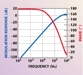
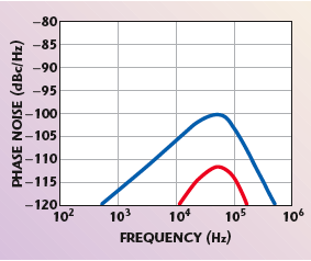
where s = j2πFmod. The term 20 • log( | 1 + G(s) | ) is the PLL FM suppression. It has been calculated for the fixed and tunable PLLs. The phase term of (1 + G(s)) is also calculated. The results are shown in Figures 14 and 15. There is approximately a 100 dB FM suppression at 500 Hz. Measurements of this level are difficult, then practical measurements were made for Fmod = 20 kHz. The measured FM suppression was 37 to 39 dB for both PLLs. These are approximately equal to the simulation results.
Conclusion
A practical airborne frequency synthesizer design is presented. A hybrid synthesizer architecture improves the chip phase noise by 8 dB. The optimal practical synthesizer architecture rejects all spurs from different sources to levels less than –64 dBc. Their levels are calculated and ways to reject spurs are discussed. An optimal power supply unit architecture permits the design to achieve high efficiency, low additional spurs and small volume, but there is a low additional phase noise from the power supply in the 300 to 600 kHz offset frequency range. The PLL FM suppression was simulated and measured.
References
1. M. Seo, J.Y. Lee and K.K. Lee, “A Varactor-tuned Oscillator with Linear Tuning Characteristic,” Microwave Journal, Vol. 45, No. 2, February 2002, pp. 100–114.

Larry Swasey
2. W.O. Keese, “An Analysis and Performance Evaluation of a Passive Filter Design Technique for Charge Pump Phase-locked Loops,” National Semiconductor Application Note 1001, May 1996.
3. D. Crook, “Hybrid Synthesizer Tutorial,” Microwave Journal, Vol. 46, No. 2, February 2003, pp. 20–38.
4. D. Colin, “Externally Induced VCO Phase Noise,” Microwave Journal, Vol. 45, No. 2, February 2002, pp. 20–41.
5. W.F. Graves, “Managing Noise and Spurious within Complex Microwave Assemblies,” RF Design, No. 7, July 2003, pp. 26–36.
Vsevolod Tanygin graduated from the radio-engineering department of Kiev Polytechnic Institute, Kiev, Ukraine, in 1986. He is currently a senior scientist with Orion Science Research Institute, Kiev, Ukraine.