

A new 28 V InGaP HBT technology has been developed for mobile infrastructure power amplifier applications that provides significant advantages in power output and efficiency compared to other technologies currently used for these devices. This 28 V process was developed from WJ Communications’ highly successful 5 V InGaP HBT process that has demonstrated very high reliability for mobile infrastructure applications. Three new power amplifiers have been developed using this new process.
The +28 V InGaP HBT process is state-of-the-art with exceptional breakdown voltage and power handling capabilities. The high breakdown voltage of the HBT was achieved with a thicker collector structure. Multiple fingers are arranged into a single building block with an emitter area around 1500 μm2. Multiple building blocks are then arrayed into a large size power HBT. Each building block has the capability to deliver 2 W of RF power in the 1 to 3 GHz frequency band. The fT and fmax of the basic HBT finger are 6.4 and 25 GHz, respectively. Lifetime tests have already been run for over 4000 hours at 315°C junction temperature with minimal beta degradation. The process has also proven to be capable of handling up to 6 dB input overdrive without failure.
In addition, a new surface mountable power DFN (Dual Flat-pack No-lead) package has been developed for these InGaP HBT devices that incorporates a eutectic die attach for the semiconductor die to minimize thermal resistance and ensure highly reliable operation.
The new +28 V ingap amplifiers raise the bar for performance and efficiency
Currently, three new amplifiers have been developed using this 28 V InGaP HBT process. They all feature high dynamic range and broad frequency range of operation in a surface-mount configuration.
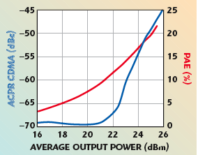
The AP601 device is a single-stage 1.8 W amplifier featuring 13.5 dB gain and high performance over the 800 to 2200 MHz frequency range with up to +32.5 dBm of output power at the 1 dB compression point (P1dB). Figure 1 shows the AP601 amplifier’s power-added efficiency (PAE) and ACPR performance vs. average output power.
In addition to using the +28 V InGaP HBT process technology, the device incorporates proprietary bias circuitry to compensate for variations in linearity and current draw over temperature. The module does not require any negative bias voltage. An internal active bias allows the AP601 amplifier to operate directly off of a commonly used single 24 to 28 V DC supply. An added feature allows the quiescent bias to be adjusted to meet specific system requirements.
The AP601 is housed in a RoHS compliant 5 × 6 mm power DFN package and typically draws 65 mA operating at +23 dBm output and 40 mA quiescent current. Input and output return losses are 10 and 8 dB, respectively. Its PAE is typically 15 percent at +23 dBm output and its output third-order intercept (OIP3) is +46 dBm for a two-tone output of +27 dBm/tone and a spacing of 1 MHz. The AP601 amplifier’s typical applications are mainly in wireless mobile infrastructure and as final stage amplifiers in repeaters.
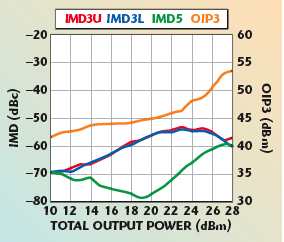
The AP602 high dynamic range 4 W amplifier is also a single-stage amplifier that operates from 800 to 2200 MHz but features a gain of 13.7 dB and up to +36 dBm of P1dB power. Its basic configuration is similar to the AP601; however, it draws 120 mA operating at +27 dBm output and 80 mA quiescent. Its OIP3 is +49 dBm and its PAE is 15 percent at +27 dBm output. Figure 2 shows the AP602 amplifier’s IMD and OIP3 characteristics.
The third amplifier in the family is the AP603 7 W device. This amplifier is also a single-stage device that operates from 800 to 2200 MHz. The AP603 features 12 dB of gain with up to +37.5 dBm of P1dB output power.
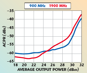
The AP603 amplifier has a 14 percent PAE at +30 dBm output and a +49 dBm OIP3. It draws 255 mA at +28 V at a power output of +30 dBm and 160 mA quiescent current. Its input and output return losses are 10 and 6 dB, respectively. Figure 3 shows the AP603 amplifier’s ACPR performance vs. its average output power.
All three new amplifiers are targeted for use as pre-driver and driver stage amplifiers in wireless infrastructure applications where high linearity and high power is required. This combination makes these devices an excellent choice for next generation multi-carrier 3G mobile infrastructure applications. Additional information may be obtained by contacting sales@wj.com.
WJ Communications Inc.,
San Jose, CA (800) 851-4401,
www.wj.com.