
For specific applications, there is a need for materials or composite structures which can reflect and/or absorb the electromagnetic (EM) energy incident upon them in a desired or controllable fashion. Such reflective EM absorbing/reflecting materials1-3 are useful in designing smart radar cross-section (smart RCS) surfaces and radio frequency identification (RFID) tags.4,5
The traditional RCS-control technique uses radar absorbing materials (RAM). Its performance can be augmented by introducing in the RAM-treated surface an active matrix made of inexpensive semiconductor diodes as proposed here. This matrix produces a pulse modulation (depicting the desired binary pattern) on the backscattered microwave energy.
The concept of facilitating such modulating capability in an electromagnetic reflecting surface is also useful in designing RFID tags.4,5 The underlying operation is as follows: An interrogator illuminates the tag and the backscattered response from the tag is sensed for identification. The information contained in the backscattered energy, defined as the RCS of the tag, is preset to present a desired (binary) code. This can be done by implementing an active (code-emitting) characteristic in the tag composition, using a set of active devices or materials that are biased in such a fashion as to yield certain changes in the reflective and/or absorptive properties of the tag, leading to a reflection in an encoded fashion. The interrogator (ITR) can decode/demodulate the received data facilitating a robust positive RFID on the tag. This technology, in general, can use a frequency in the megahertz through gigahertz region of the RF spectrum. However, shorter wavelengths would enable a significant RCS/ 2 ratio.
The tag corresponding to a responder (RSR) in the proposed effort needs on-board power for the biasing scheme. However, the associated power consumption is rather low since there is no active transmitter on-board. Furthermore, the on-board biasing of the tag and "tuning" the interrogator to selectively sense the adopted encoding would increase the functional range of the tags. Hence, the tags in question do not have to operate in close proximity to the interrogator (as otherwise required in passive tag systems).

Details of a prototype developed and tested at microwave frequencies are presented in this article in reference to the two applications described above. They include surfaces that enable a controlled (modulated) RCS of radar targets and surfaces useful in RFID tag designs.
In order to design a device that presents a varying reflection coefficient to an incident EM wave, such as microwaves, a surface which has switchable microwave reflection properties is needed, with two distinct and controllable modes of operation - high and low reflectivity. This can be achieved by having a passive material that changes its EM properties (such as dielectric phase to conduction phase or vice versa) when an electrical signal excites it3,6-9 or by having an array of active devices (such as semiconductor diodes), which can be switched to change the bias conditions.
The control method proposed here refers to the second method. It uses a set of active devices that are lightweight and small-size diodes that can be operated with low power consumption. A diode is ideally suited for this application since it possesses two distinctly different conduction states (on or off) that are dependent on the DC bias imposed.
The active surface can be made of a composite using a set of elements, as illustrated in Figure 1. The RAM shown as a substrate is needed only in RCS-control applications and can be omitted in RFID tags.
When an interrogator illuminates the test surface at a microwave frequency, the backscattered energy from the surface can be made to depend on the active state of the diodes on the PCB as decided by the binary input (a forward bias or a reverse bias) imposed by an erasable programmable read-only memory (EPROM) encoder. When the diodes are forward biased, they form a parallel set of grids (that is, a grille structure); for reverse bias conditions, they are open circuited, as illustrated in Figure 2.

In essence, the parallel grids constitute a diffraction grating. Suppose the E-component of the incident wave is parallel to the "grille rods" emulated by the forward-biased diodes. The E-field will be "shorted out," whereas an E-component perpendicular to the "grille rods" will pass through the grille. When the diodes are reverse-biased, they offer a large impedance and do not emulate the parallel set of "grille rods" as above. As such, both horizontal and vertical components of the E-field will pass through the diode array almost uninhibited. Thus, the forward- and reverse-bias conditions of the diodes emulate and present two distinct surface states (grille and no-grille) to an incident EM wave. This property is used beneficially to make a surface for a controlled-RCS or an RFID tag as proposed here. The present concept of emulating an "active" diffraction grid somewhat conforms to earlier reported studies.10-13
The semiconductor diodes (switching diodes or Schottky-barrier diodes) act as a set of current-source driven elements, which is controlled by the operation of the EPROM encoder chip (such as a Holtek HT12E). This chip provides the necessary modulation according to a preset binary message. The diode array plus the encoder arrangement used in the test study is illustrated in Figure 3.

The experimental studies performed indicate that Schottky-barrier diodes, traditionally intended for detector or mixer circuits at microwave frequencies (such as HSCH-6312), yield optimum performance. Also, a much cheaper diode (like the switching diode 1N4148) was found to yield a comparable performance and forms an effective substitute for the expensive Schottky diode.
The prototype of the surface constructed for the test study consists of four diodes arranged horizontally between a pair of parallel copper traces on a PCB (Figure 4). The anodes of the diodes are tied together via a common bus to the supply voltage. Similarly, the cathodes are connected together and terminated at the collector of the 2N222 BJT (Q1 ) driver. Other interconnections are made with copper traces on the PCB as necessary.

Placing a reflecting surface (such as an aluminum foil) behind the diode grid increases the detected backscattered energy. If the spacing between the diode and the metallic background is made equal to a quarter wavelength ( /4), the total phase shift from the diode grid to the metal background and back would be /2 or 180°. Also, because of the phase shift of the metal short circuit, which is also 180°, the total phase shift experienced by the signal is 360°, that is, in phase with the original reflection, thus enhancing the detected signal. Such quarter-wave window concept is well known in the design of the so-called Salisbury screens.3
The EPROM encoder used to generate the binary pattern can be set to develop a 12-bit parallel code, the binary state of which corresponds to either the digital inputs connected to ground or to the supply voltage. A DIP switch can be used to write a code on the EPROM. The encoder chip also converts the parallel code to a serial code, which is preceded by an additional synchronization bit with the input binary state modulated into a certain pulse-width. Thus, the chip provides a pulse-width modulated serial code, which is sent to the diode bank for forward or reverse biasing via a current-sinking transistor (BJT). That is, the base of the BJT is connected to the output of the encoder, so that the current that the transistor will sink is modulated according to the desired message. The BJT, in turn, applies the corresponding bias to the diodes, following the binary pattern given by its current sinking function.
The data rate at which the encoder chip should generate the required modulation (binary word) can be set by the clock rate, which can be chosen with an appropriate choice of supply voltage (Vo ) and the resistance (Rosc ). An experimental study indicated that data rates as high as 10 kHz can be achieved with a supply voltage as low as 2.5 V with the encoder chip used. Hence, a standard quarter-size 3 V battery (such as type 2032) was used in the test. The flexibility in supply voltage and choice of battery type allow the final design of the test surface to assume a credit-card size (as may be required in RFID applications) and the entire modulation circuit plus the diode array can be fabricated in wafer form using VLSI fabrication.
It was further observed in the test study that the amount of current driven through the diode band significantly influences the effectiveness of the diodes in emulating an active grille and in altering the reflected RF energy. The required level of the diodes bias current for optimum performance can be set by the base resistor R1 in conjunction with the supply voltage. The emitter resistor R2 is used to limit the on-state condition allowing a minimal emitter/collector current at which the diode forward resistance approaches almost to its lowest attainable value. This choice of bias current conserves the power consumption and hence increases the battery life.
Transmit-Receive Test Arrangement
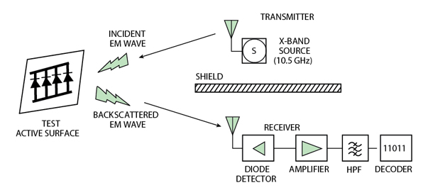
The interrogator unit used in the test set up consists of a 10.5 GHz oscillator and a patch antenna that illuminates the test surface. The relevant bistatic (transmit-receive) interrogator arrangement is illustrated in Figure 5. The transmitter of the interrogator unit radiates a continuous wave and the receiver patch antenna senses the backscattered energy from the test surface. This backscattered signal is demodulated by a diode detector, which can be modeled as a current source whose output current (I) is determined nonlinearly by the input voltage (V), according to the I-V characteristics specified by
I(V) = Is (eaV -1)  Is eaV
For small RF input signals, the nonlinear relationship can be expanded in Taylor-series around the quiescent bias voltage Vo. Hence, ignoring the higher order terms, it follows that
I(Vo + V)≈
I(Vo + [dI/dV]V + [1/2][dI/dV]V2
The first term in the expanded expression of the current represents the DC part that biases the diode; the second term is the output current, which is directly proportional to the input voltage and weighted by the linear conductance (dI/dV). The last term is the diode current representing the square-law detected part of the microwave signal. This detection process leads to a demodulated low frequency signal envelope, which can be amplified (to approximately 0 to 5 V range) and sent to a decoder chip (such as a Holtek HT12D). The decoder, in turn, generates latched digital outputs corresponding to the transmitted code from the active test surface.
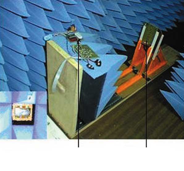
In RFID applications, these digital outputs can be used to ascertain a positive RFID of the active test surface, emulating an RFID tag. In RCS-control applications, the detected (encoded) envelope would correspond to a set of (preset) deceptive pulses from a target supposedly treated with the test active surface. When received by the enemy radar, such pulses would cause false alarms enabling an electronic counter measure. The photograph in Figure 6 shows the test-range used in the experiments which were made in an anechoic chamber.
Design Considerations
RFID Application of the Test Active Surface
The crucial consideration in the design of the proposed test active surface, especially for RFID applications, is its power consumption. The active devices, diode bank, BJT driver and encoder that constitute the active surface use an on-board battery. As such, necessary power is consumed in emulating the on-off grille, which is exposed to incident microwaves enabling a modulated backscattered energy as explained earlier.
The RFID-tag with an active on-board circuitry could be designed to operate over a desired range of conditions. The limitation, however, is the life span of the battery. Such tags must be placed for immediate use without being subjected to prolonged shelf-storage when made as disposable types. But the tag-card design can also be modified with a replaceable on-board battery in non-disposable versions.
The proposed active surface in RFID tags operated at microwave frequencies allow the use of narrow interrogator antenna beams, thereby facilitating an EM foot-print of RFID search confined to a smaller area. Such well-defined coverage will permit the system to recognize only one tag at a time, thus avoiding collisions of multiple tags (if present), which otherwise may cause data corruption and false identifications.
This relevant method is highly compatible with security purposes as required for personal ID cards that can be sensed without the need to swipe the card for an entry through a door, for example. The tags can also be mounted on cars for secured gate-entry or passage through a prepaid toll station. When the tag is worn by a person or mounted on a car at an assigned location, the interrogator can be placed to cover a foot-print of volume within which the tag can be sensed robustly. Furthermore, the tag can be designed to have an operating range of approximately one to two meters and its operation will remain transparent to the user.
Since the preset stored-code cannot be captured outside the foot-print of the interrogator, the tag in question will allow only those personnel or cars to enter or exit the restricted areas with the interrogator examining the unique identification code assigned to each tag on the person or car.
The interrogator part consists of a microwave transmitter and receiver kept separated by a few inches, but adequately shielded from each other so as to form a bistatic arrangement. In the test study performed, a 10.5 GHz Gunn oscillator was used as the transmitter (interrogator) and the receiver that senses the modulated backscattered microwave from the active surface (tag) consisted of electronics, as depicted in the block schematic of Figure 7.

The small separation between the transmit-receive (T/R) units is consistent with the small size of the T/R module to be strategically placed, with respect to the expected tag location, for maximum range of operation. A larger separation between T/R units would require a lengthy interconnection cable, susceptible to 60 Hz ambient noise. This has to be suppressed prior to processing the received signal.
Shielding between T/R units is incorporated in order to overcome any direct coupling between transmit and receive antennas. If such a coupling exists, the receiver patch antenna will pick up a portion of the transmitted CW energy. This CW interference upon detection will present a wandering DC level, which is undesirable for the operation of the subsequent amplifier stages. Therefore, any such DC component should be suppressed by using an appropriate clamping circuit.
The first amplifier section provides adequate gain and enables the demodulated signal to acquire a sufficient level so that any additional noise contributed subsequently may not significantly drown the signal in noise. The second amplification stage combines an active high pass filter whose cut-off frequency is chosen such that its output resembles closely the encoded waveform without any low frequency artifacts.
The next section of the receiver unit does the pulse-shaping of its inputs into a clean digital waveform limited at a constant output level. This amplitude-limiting function is necessary since the final digital output should be of constant amplitude regardless of the fact that the demodulated signal may vary in amplitude depending on the relative location (range) of the tag with respect to the interrogator. In addition, the pulse-shaping and amplitude-limiting circuits provide a digitized output devoid of any distortions in the waveform, caused by the preceding amplifier and filtering stages.
The output of the pulse-shaping circuit will swing approximately between the positive and negative supply voltages (±5 V), and a Schmitt trigger stage that follows limits all outputs approximately to +5 V and does not allow the negative signal swing. The output of the limiter stage feeds a decoder chip, which can be connected to a set of LEDs displaying the transmitted code for monitoring.
In the constructed test circuit, the decoder circuit has eight address inputs and four latched outputs. As a result, when the incoming serial code matches all the address bits, the decoder outputs the four-bit data message to the latched digital output pins. Thus, the message is retained until a new (different) code is received. A typical data set at the active surface (tag) and the output of the digital stage at the interrogator receiver, as captured on a CRT screen, is shown in Figure 8.
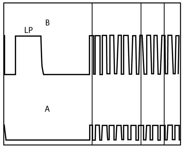
The CRT traces in the figure show that the binary data (indicated as A) applied at the active surface (tag) is reproduced faithfully (shown as B) by the receiver with the exception of a large additional pulse (marked LP) before the start of the data burst. This extra pulse is generated by the transient response of the filter and is not a part of the data. However, since the pulse-width of the extra bit (LP) is distinct from that of the data, the decoder circuit ignores it. As such, the presence of LP will have no bearing on the functionality of the decoder. Thus, the entire test system as conceived was seen to function successfully with the tag message identified on the LEDs.
The interrogator of the RFID unit described above has to be compliant with Part 15 of the FCC Rules and Regulations. Such compliance will allow the unit to be operated without an individual license when the transmitter complies with both subparts B and C of Part 15 Rules and Regulations. In particular, for microwave operation, the unit will have to comply with emission limits given in section 15.245b. As a result, the maximum emission at the fundamental frequency should be below 2500 mV/m and the maximum emission at the harmonics must be less than 25 mV/m. Since the device will intentionally generate fields in the direction of personnel, it must be guaranteed that such operation does not present any health hazard. According to Part 1 of the FCC Rules and Regulations, a generated field will be deemed safe if the exposure levels and the durations of exposure are in compliance with the limits given in 1.1310, namely, the power density in any area of the illuminating field has to be below 5 mW/cm2 .
RCS-control Application of the Test Active Surface
As indicated in earlier sections, the design of the test active surface can also be modified to suit its application as a smart facet on a target, which offers a controlled-RCS when subjected to an illumination from enemy radar. The corresponding backscattered echo would then contain a binary modulated artifact in its waveform that could confuse the illuminating radar. Furthermore, the active surface can be embedded in a substrate of radar absorbing material of different types.3,13-17 A distinguishing feature of the test surface when deployed for active RCS-control applications is that there may not be any power-budget restrictions on energizing the active elements involved. This is because the vehicle (such as an aircraft) will have sufficient power to energize the entire set of patches of the test surface attached to it to achieve the controlled-RCS.
Thus, the proposed method (akin to that described by Chambers and Tennant12 ) provides a strategy to enable a controlled-RCS technology via actively manipulated EM scattering attributes. This technique can offset some of the trade-off considerations on weight and thickness penalties versus RAM-based RCS control. Further, selective use of RAM plus the proposed active surface at certain optimum locations15,16 on the target geometry can pay off with significant RCS reduction benefits.
Conclusion
This work is a pilot study carried out towards developing an active surface compatible for RFID and smart/controlled-RCS realizations. The results obtained with a laboratory version of the test active surface provide an encouraging impetus for future studies and improvements on the test surface investigated. An interesting sequel of the effort corresponds to switching each of the diodes used in the test surface independently, so that the total diode array, configured with a prescribed pattern of on- or off-states at any given time, constitutes a structure of spatially-switched binary grid elements. This spatial on-off pattern of the diodes, together with a temporal modulation imposed, would form a "two-dimensional (space and time) bar-code." This can lead to more comprehensive data representation in terms of size, security and details in RFID tags; when adopted in RCS-control methods, it can introduce severe jamming artifacts in the echo signatures of enemy radar. Relevant studies are in progress.
References
1. A.F. Harvey, Microwave Engineering , Academic Press, London, England 1963, pp. 601-605.
2. H. Jasik (Ed.), Antenna Engineering Handbook , McGraw-Hill Book Co., New York, NY 1961, Chapter 32, pp. 35-40.
3. P.S. Neelakanta, Handbook of Electromagnetic Materials: Monolithic and Composite Versions and Their Applications , CRC Press, Boca Raton, FL 1995.
4. M. Reynolds, "Microwave RFID: Passive Scattering and Active Transponders," http://hyaku.www.media.mit.edu/~mat/scattering.html, 15 September 1999.
5. R.J. Jackson, "An Overview of RF Tags," http://home.att.net/~randall.j.jackson/rfid-overview.html, 2 October 1999.
6. P.S. Neelakanta, J. Abello and C. Gu, "Microwave Reflection at an Active Surface Imbedded with Fast-ion Conductors, IEEE Transactions on Microwave Theory and Techniques , Vol. 40, No. 5, May 1992, pp. 1028-1030.
7. M. Hamid, "Polyconductor Beam Power Sensor," International Journal of Electronics , Vol. 71, No. 2, February 1991, pp. 363-381.
8. R.C. Dempsey and R. M. Bevensee, "The Synaptic Antenna for Reconfigurable Array Applications," 1989 IEEE Antennas and Propagation International Symposium Digest , 1989, pp. 760-761.
9. P.S. Neelakanta and D. De Groff, "Smart Shielding May Modify Performance to Fit," EMC Technology , Vol. 9, No. 3, May/June 1990, pp. 25-29.
10. S.K. Chatterjee, R. Chatterjee and D.V. Giri, "Simulated Plasma at X- and K-bands," Journal of the Indian Institute of Science , Vol. 52, 1970, pp. 225-246.
11. S.K. Chatterjee, R. Chatterjee and D. Sunderarajan, "Some Investigations on Artificial Plasma at Microwave Frequencies," Journal of the Institute of Engineers (India), Vol. 49, 1968, pp. 9-14.
12. B. Chambers and A. Tennant, "Characteristics of Phase Switched Screens in the Presence of Pulsed Radar Signals," Proceedings of the 2002 Antennas and Propagation Society International Symposium , June 16-21, 2002, San Antonio, TX, Vol. 3, pp. 380-383.
13. S.K. Chatterjee, H. Kaushal and R. Chatterjee, "A Two-dimensional Array Absorber for Microwaves," Journal of the Indian Institute of Science , Vol. 51, No. 1, January 1969, pp. 103-113.
14. E. Meyer, H. Severin and G. Umlauft, "Resonazabsorber für Elektromagnetische Wellen, Z. Phy.," 138, 1954, pp. 465-477.
15. S.K. Chatterjee, P.S. Neelakantaswamy and R. Chatterjee, "Measurement of Back Scattering Cross-sections of Metallic Bodies of Revolution at X-band," Journal of the Institution of Engineers (India), Vol. ET-49, 1969, pp. 87-93.
16. P.S. Neelakantaswamy, D.K. Banerjee and T. Parthasarathy, "Modified Radar Cross-section of a Dielectric Cylinder with Conducting Circumferential Loop Loading," Archiv. Elek. u-Übertrg ., Vol. 27, No. 4, April 1973, pp. 192-193.
17. C.A. Grimes, "Broadband EMC Absorbing Materials, 1993 International Symposium on EMC Record , August 9-13, 1993, Dallas, TX, pp. 245-249.
P.S. Neelakanta received his B. Eng. degree from the University of Madras (India), in 1966, his M. Eng. degree (with distinction) from the Indian Institute of Science, Bangalore (India), in 1968, and his PhD degree from the Indian Institute of Technology, Madras (India), in 1975. He is currently a professor of electrical engineering at Florida Atlantic University (FAU), Boca Raton, FL. His specializations and research interests include microwaves, EM theory, bioelectromagnetics, dielectrics and electromagnetic properties of materials, shielding, antennas, bioelectromagnetics stochastical communication theory, radar signals/clutter, ATM, wireless and wireline telecommunications, next generation networking, neural networks, bioinformatics and information-theoretic modeling. He has published over 150 papers and five books and is a Fellow of the IEE (UK) and a Chartered Engineer (UK).
Anthony K. Stampalia received his BSEE degree (summa cum laude) from Florida Atlantic University (FAU) in the Spring of 2000. He currently works for Motorola in Plantations, FL, designing the receiver section of the iDEN radio. His research interests include RF/analog design.
Dolores De Groff received her master's degree in 1990 and her PhD degree in 1993 from Florida Atlantic University (FAU). She is currently an associate professor of electrical engineering at FAU. Her research interests include radar, neural networks and analytical methods.