
The performance of communication systems, in both space and ground segments, is degraded by the nonlinearity of the power amplifiers that are operated in saturation to obtain higher efficiency. Linearizing is the technique used to improve the performance of communication systems when power amplifiers are operated in saturation. The linearizer reduces the need to trade off efficiency for linearity by allowing a given linearity to be achieved with less power back-off.
Various types of pre-distortion linearizers have been reported.1,2 Schottky diode-based pre-distortion linearizers have shown considerable promise because of their simplicity and compactness.3 This article describes the design, development and test results of a novel pre-distortion linearizer using the nonlinearity of Schottky diodes. Such a linearizer generates a gain change and phase shift as a function of input drive, and compensates for the nonlinear behavior of the amplifier.
The topology presented here is highly versatile in the sense that it can generate different combinations of nonlinearity, with adjustable slopes, and can therefore be tailored to match different device behaviors encountered in practice. These combinations are as follows:
With increasing RF power to the linearizer:
-
 S21 decreases and |S21| increases.
 -
S21 increases and |S21| increases.
These two cases are required to linearize traveling wave tube and solid-state power amplifiers (TWTA and SSPA). The following two cases can also be obtained but are not relevant in linearizer design:
-
S21 decreases and |S21| decreases.
-
S21increases and |S21| decreases.
Using this topology, an S-band linearizer has been designed and developed to linearize an S-band SSPA. The improvements are as follows:
- For the same output power, the gain compression is reduced from 3.2 to 0.8 dB.
- At the same output power level, the total phase shift improves from 6.2 to 1.0°.
- The third-order modulation product (IM3) is improved by 3.5 dB at the 1 dB output power back-off and 8.5 dB at the 2 dB output power back-off.
Circuit Topology
The circuit topology of the linearizer presented here is shown in Figure 1 . The input signal is divided into two equal amplitude signals; one is fed to a distortion generator and the other is attenuated and phase shifted. The two signals are then recombined in a 3 dB power combiner. The magnitude of the ratio of output and input signals is:

The phase of the output signal is given by

where
Knl = attenuation factor in the nonlinear arm given by
Knl = knlo + knl (pin) (3)
 = phase angle between the two signals at the output port given by
=  o + (pin) (4)
where
knlo, o = values corresponding to the small-signal condition and knl(pin)
(pin) = power dependent values
From Equations 1 and 2, it is clear that the variation in magnitude and phase of S21 as a function of input power can be controlled by selectively choosing the values of KL, knlo, o. By plotting these two equations, it can be shown graphically that any combination of magnitude and phase variation can be achieved by selecting the values of these three parameters.
Distortion Generator Circuit
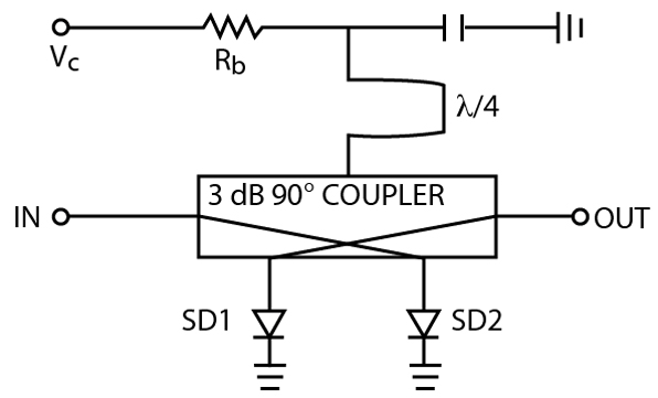
A reflection type distortion generator has been designed. The circuit schematic is shown in Figure 2 . This attenuator is built around a 3 dB, 90°, hybrid Lange coupler. Two beam-lead Schottky diodes SD1 and SD2 (HSCH 5315) are used. The control voltage Vc is applied to the diodes through the bias resistor Rb and a  /4 transmission line.
The magnitude of the insertion loss of this distortion generator circuit is

and the phase of the insertion loss is
where
Ro = characteristic resistance of the source and load
Rd = equivalent dynamic resistance of the Schottky diode that depends on the voltage across the diode and the RF power applied to the circuit
Cd = equivalent capacitor of the diode, which remains nearly constant over the applied RF power range
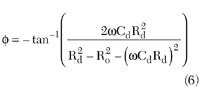
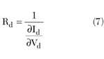
Figure 3 shows the variation of phase and magnitude of the insertion loss as a function of the dynamic resistance of the diode. When an RF power is applied to the input of this circuit, the average current through the resistor Rb increases because of the nonlinearity of the diodes. Therefore, the voltage across the diode decreases. The diode dynamic resistance is given by4
where

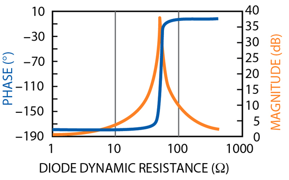
From this equation, it is clear that the diode dynamic resistance Rd increases with increasing RF input power. The rate of change of the diode voltage with the change of RF power depends upon the value of the bias resistor Rb. The rate of Rd increases as a function of the RF power level and can be controlled by selecting the value of the resistor Rb.
Therefore, from Equations 5 and 6, it is clear that the magnitude and phase of the insertion loss of this circuit change with the RF input power variation.
Linearizer Realization
In the case of a communication transponder, the gain compression and phase change of an SSPA are nearly 3 dB and 20°, respectively. The corresponding parameters for a TWTA are nearly 6 dB and 35°. Therefore, the gain expansion of the linearizer should be 3 and 6 dB, and the phase change should be nearly 20° and 35° but in opposite direction for the SSPA and TWTA, respectively.

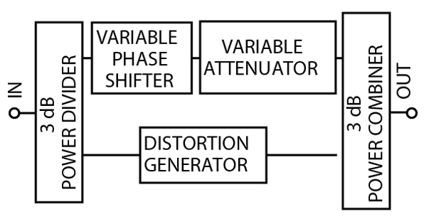
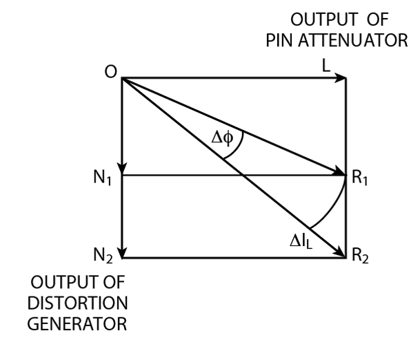
The capacitance Cd = 0.15 pF for the diode HSCH-5315 used with the change of bias to the distortion generator, when the dynamic resistance of the diode changes from 50  to its maximum, then a phase increase of nearly +5°, is practically achieved, as shown from Equation 6. Therefore, the distortion generator alone is not able to linearize the SSPA and TWTA. The schematic of a versatile linearizer, to linearize a wide range of nonlinearity of SSPA and TWTA, is shown in Figure 4. Here, the input signal is divided into two equal amplitudes with a 90° phase difference. One signal passes through a linear arm and the other through a nonlinear arm. The two signals are then recombined with an in-phase combiner. The nonlinear arm is a distortion generator based on Schottky diodes SD1 and SD2 (HSCH 5315) and the linear arm is a reflection type variable attenuator with PIN diodes D1 and D2 (HPND 4005). The vector diagram of the output of the linear and nonlinear arms is shown in Figure 5. In the small-signal case, the vectors corresponding to the linear and nonlinear arms are OL and ON1, respectively. As the RF input is increased, the vector ON1 increases to ON2, while the vector OL remains unchanged. Therefore, the resultant output vector changes from OR1 to OR2. From this vector diagram, it is clear that the magnitude of the resultant vector increases by
  IL and the phase of the resultant vector decreases by .
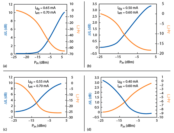
An S-band linearizer has been designed and tested. The measured variation of magnitude and phase of the insertion loss is shown in Figure 6 for different bias settings of the attenuator (Iatt) and distortion generator (Idg). The graphs show the changes in value with respect to the small-signal case. These curves show that different combinations of magnitude and phase changes with input RF power can be achieved by varying two bias voltages. In particular, a decrease of insertion loss and phase with RF power is required to linearize the SSPA and TWTA (a result achieved by setting the dynamic resistance to be greater than Ro).
Alternatively, the bias given to the PIN attenuator could be such that the dynamic resistance of the PIN diodes is less than Ro.4 In this case, an increase of RF power will produce a decrease in insertion loss, and the insertion phase will also increase. This behavior of the linearizer may be sometimes required to linearize the SSPA and TWTA.
For the sake of completeness it can be shown that, if the bias applied to the Schottky diodes is such that the dynamic resistance of these diodes is less than Ro, the other two combinations of insertion loss and insertion phase (that is, 1) increase of insertion loss, decrease of insertion phase and 2) increase of insertion loss, increase of insertion phase) can be achieved.
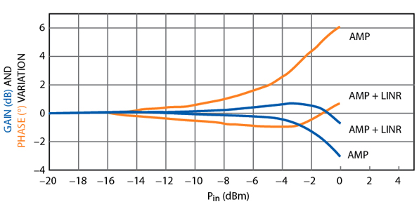
The MIC assembly diagram of the linearizer is shown in Figure 7 . This linearizer was evaluated with an S-band SSPA. The improvement in gain compression and total phase shift is shown in Figure 8 . The gain compression decreased from 3.2 to 0.8 dB at the nominal output power. The maximum total phase shift decreased from 6.2° to 1°.
Figure 9 shows the improvement in third-order intermodulation product for different output power back-offs. It shows that a 3.8 dB IM3 improvement at 1 dB output back-off and on 8.7 dB IM3 improvement at 2 dB output back-off were obtained.
Conclusion
It can be concluded that this topology of the pre-distortion linearizer has the capability to linearize a wide range of phase and amplitude nonlinearities. The main features of this linearizer are its versatility. The same linearizer can be used for SSPAs and TWTAs. It is easily tunable. Only bias voltages and resistors are adjusted for different SSPAs and TWTAs, and its size, weight, reliability and power consumption, which are particularly relevant in space applications, are improved.

References
1. R. Inada, et al., "A Compact 4 GHz Linearizer for Space Use," IEEE Transactions on Microwave Theory and Techniques , Vol. 34, No. 12, December 1986, pp. 1327-1332.
2. C.T. Rodrigo, et al., " MESFET Nonlinear Applied to Pre-distorsion Linearizer Design," IEEE International Microwave Symposium Digest , 1992, pp. 955-958.
3. K. Yamauchi, et al., "A Microwave Miniaturized Linearizer Using a Parallel Diode with a Bias Feed Resistance," IEEE Transactions on Microwave Theory and Techniques , Vol. 45, No. 12, December 1997, pp. 2431-2435.
4. J. Millman and C.C. Halkias, Integrated Electronics , McGraw-Hill, 1988.
 S.C. Bera obtained his M. Tech. degree in radio physics and electronics from the University of Calcutta, and joined the Indian Space Research Organisation, Ahmedabad Centre, in 1994. Since joining ISRO he has been involved in many payload projects like INSAT-2C, 2E, INSAT-3A, 3E and GSAT series of spacecrafts. Presently he is deputy project manager for SSPAs for the INSAT-3E and SATNAV payload project. His field of work is design and development of SSPAs, channel amplifiers, linearizers, attenuators and phase shifters.
 P.S. Bharadhwaj obtained his bachelor's degree in electrical engineering from Gujarat University, India, in 1982, and his master of technology degree from the Indian Institute of Technology, Madras, in 1984. He has been with the Indian Space Research Organization's facility in Ahmedabad, India, since 1986. His areas of interest include satellite channel amplifiers, power amplifiers and linearizers.
 R.V. Singh obtained his B. Tech. (EE) degree from GB Pant University of AG and Technology, Pantnagar, Nainital, in 1972. He joined the Experimental Satellite Communication Earth Station (ESCES) at Ahmedabad in October of that year, which subsequently became the Space Applications Centre, ISRO. He started his career as a designer of low noise amplifiers (LNA) for satellite communication applications. He has designed various LNAs with state-of-the-art performance that have been used in various projects of ISRO. Presently he is group director, Power Amplifier Group, at the Space Applications Centre. He is a life member of the International Society for Hybrid Microelectronics and Packaging-India chapter.

 V.K. Garg received his B. Tech. degree in electronics and communications from IIT, Madras, India, in 1970. He joined the Experimental Satellite Communication Earth Station (ESCES), Ahmedabad, in July 1971, after spending one year at the BARC Training School (14th batch). Since 1971, he has been involved in all major communications satellite projects of ISRO, including SITE, STEP, APPLE, INSAT-1, INSAT-2, INSAT-3 and now INSAT-4 series of spacecrafts. He was associate project director for INSAT-2C and INSAT-2D communication payloads. Presently he is deputy director, Satcom Payload Technology Area, at the Space Applications Centre, Ahmedabad.