
Recently, there has been an increasing interest in studying microstrip lines with various periodic structures that prohibit wave propagation in certain frequency bands, including photonic bandgap (PBG) and DGS.1-10 Each periodic structure has its own properties and advantages. DGS, which is realized by etching only a few areas on the ground plane under the microstrip line, is also a kind of periodic structure.4
In the microwave region, PBG structures have been used in the design of antennas, cavities, frequency-selective surfaces and many other structures. However, most of these PBG applications are limited to providing deep and wide stopband performance of the circuits.1-2 Meanwhile, DGS provides a significant advantage by extending its applicability to other microwave circuits, such as filters, dividers, couplers, amplifiers and oscillators.3,7,8,9 PBG has also been used in filter designs to improve their stopband performance by rejecting the higher order passbands, due to its inherent stopband behavior. Both PBGs and DGS have been very effectively used to improve the power-added efficiency (PAE), which is the most crucial factor in power amplifier design, by terminating the harmonics adequately. However, the previous DGS design methods for various microwave circuits have employed not its equivalent circuit but EM-simulated S-parameters for a specific DGS circuit. Since the previous design methods are not based on its equivalent circuit, time-consuming iterative design procedures are required to accomplish the design goals. In this article, a new accurate equivalent circuit model is proposed, which can be applied to the design of a microwave circuit with circuit.7,11,12 Thus, a microwave circuit including the proposed DSG equivalent circuit can be optimized to meet the specifications.
In order to show the efficiency of this method for the design of various microwave circuits, using the proposed equivalent circuit of the DGS, a harmonic rejection low pass filter with a 4 GHz cutoff frequency is designed with a circuit optimization procedure. Simulation and measurements for the optimized low pass filter are compared. As another example of the application of a DGS equivalent circuit, a very efficient design method is presented for the purpose of improving the performance of a class-AB power amplifier by using the optimizing procedure for a DGS power amplifier output circuit. The presented design method employs the equivalent circuit of the DGS as a matching circuit at the output of a power amplifier. The output matching circuit, including the DGS circuit, provides the optimum load condition to obtain the maximum output power and the desirable harmonic rejection for improving the efficiency of the power amplifier. In order to show the validity of this method, a 20 W power amplifier was designed to operate at 2.11 to 2.17 GHz. Three kinds of power amplifiers have been fabricated to compare their results. The effectiveness of the proposed design method compared with the previous design method is shown by comparing performances in terms of output power, harmonic power and power-added efficiency. In addition, a comparison between the results of the conventional method of using DGS and the results of the newly proposed method was made, to disclose the efficiency of the proposed method. In addition, a novel DGS microwave oscillator is demonstrated to show a design example fully based on the proposed equivalent circuit.

Modeling Method
Along a microstrip line, DGS can be achieved by etching a dumbbell shape area in the metallic ground plane. Figure 1 shows a DGS microstrip with a unit defect, which is etched in the ground plane, and its newly proposed equivalent circuit.
A DGS unit has a cutoff frequency at a certain frequency due to the increase of the effective series inductance of the transmission line. It also has an attenuation pole above the cutoff frequency. Thus, in the equivalent circuit, the etched defect on the metallic ground plane can be modeled as a parallel LC resonant circuit with a parallel conductance. But this parallel LC resonant circuit is not sufficient to explain the effect of discontinuities on the performance of the DGS. The proposed equivalent circuit includes the parallel capacitance that is due to the relatively large fringing field at the step discontinuity plane on the metallic ground surface. Since the parallel capacitance causes a change in the characteristic impedance level and electrical length of the DGS unit section, it should be considered as part of the equivalent circuit for a more accurate modeling procedure. In order to derive the equivalent circuit parameters, the S-parameters of a unit DGS cell at the reference plane between the conventional microstrip and the DGS are calculated by EM-simulation.5-8 The S-parameters for the unit cell are simulated using Ansoft HFSS. Once the S-parameters are calculated at the cutoff frequency, the equivalent circuit parameter can be extracted by using the relation between the S-parameters and the ABCD-parameters

where
Ya = series susceptance of the π -type symmetrical two-power circuit
Yb = parallel susceptance of the π -type symmetrical two-port circuit
Then, the ABCD parameters of the π -type symmetrical two-port circuit are represented by these equivalent circuit parameters. The resulting relations between the equivalent circuit parameters of the π -type symmetrical two-port circuit and the equivalent circuit parameters of the proposed DGS circuit are given by

Since the calculated S-parameters for the unit DGS circuit are complex numbers, the resulting equivalent circuit parameters of the π -type symmetrical two-port circuit are also complex. From these relations, the equivalent circuit parameters of the proposed DGS circuit are given by

where
ω 1 = cutoff frequency of the EM-simulated results for the unit DGS circuit
ω 2 = attenuation pole location of the EM-simulated results for the unit DGS circuit
Re[Ya] = real parts of Ya
Re[Yb] = real parts of Yb
Applications to Microwave Circuits
Design of a Low Pass Filter
In order to demonstrate the effectiveness and usefulness of the proposed DGS model, an immediate and straightforward application of the proposed DGS equivalent circuit is a harmonic rejection low pass filter. By employing the proposed equivalent circuit, a three-section DGS low pass filter has been optimized to have an optimum performance in the passband and the stopband simultaneously. The cutoff frequency of the designed three-section DGS low pass filter was chosen to be 4 GHz. Figure 2 shows the optimized DGS low pass filter schematic and the element component values. The design variables for optimization are the proposed equivalent circuit parameters of the unit DGS cell and the transmission line parameters for cascading the unit DGS cells. The conductance value in the equivalent circuit does not need to be considered as a design variable during the optimization.
Because the designed DGS low pass filter is symmetric, with the input and output DGS circuits identical, it can be separated into two parts. In order to implement the optimized DGS low pass filter from its equivalent circuit, each individual section should be fabricated according to the corresponding optimized unit DGS cell. The input and output sections of the designed DGS low pass filter schematic are implemented with a physical DGS cell with conventional 50 Ω microstrip lines at both ends leading to a parallel capacitor Cp = 0.28774 pF. The intermediate section was designed with 32 Ω microstrip lines at both ends. When these unit DGS cells are used in the optimization of the entire filter, these microstrip lines are eliminated by deembedding the DGS equivalent circuit. As a result, for the final filter design, the input and output sections have transmission lines of 29 and 16 Ω at either end, while the middle section has transmission lines of 16 Ω at both ends. The substrate used in the EM-simulation of the unit cells was an RT/Duroid 5880, 31 mil thick with a dielectric constant ε Ρ = 2.2. The results of the EM-simulation agree relatively well with those of the analysis of the equivalent circuit.
Design of a High Power Amplifier with DGS Circuit
The examples of a high power amplifier design will show the usefulness of the proposed equivalent circuit of a unit DGS cell for applications to various RF and microwave circuits. The main design objectives of a power amplifier are high output power saturation and efficiency with excellent linearity. However, it is hard to implement a power amplifier to satisfy these requirements simultaneously. There is some trade-off between these design objectives in the design of a power amplifier by adjusting the bias of the active device. High efficiency is an important characteristic of a power amplifier that allows for smaller and lighter power sources and reduces the cooling requirements. High efficiency power amplifiers have been investigated and implemented by controlling or terminating the output harmonics from the nonlinear active devices biased in class-B or class-AB.13-15
One technique, widely used previously for controlling the harmonics of a power amplifier, is harmonic shorting by the appropriate choice of a quarter-wavelength open-circuited stub with an RF shorting chip capacitor. A DGS cell has been used for this purpose in the output section of the power amplifier configured only as a filter for harmonic rejection.3 The design example of a high power amplifier, presented in this article, has also employed DGS circuits to achieve improvement in efficiency performance. But it differs in the design method compared with that of the previous techniques with DGS circuit. The present design method utilizes the equivalent circuit of the DGS section to optimize the output circuit. By using the DGS equivalent circuit, the optimized output matching circuit, which provides the optimum reflection condition at the fundamental frequency and an excellent rejection of the second harmonic, can be realized. A 20 W LDMOS device was used to implement a class-AB power amplifier operating at 2.11 to 2.17 GHz. The LDMOS device for the implemented power amplifier is an MRF21030 from Motorola. Two choke air-coil inductors that are self-resonant at the fundamental frequency can be used in the bias supply. In order to tune the harmonics, especially the second one, these choke inductors should be considered as a low impedance element to provide a harmonic short via shorted capacitors. However, this is not sufficient in power amplifier applications. Figure 3 shows the schematic of the output circuit including the DGS circuits for a class-AB power amplifier.
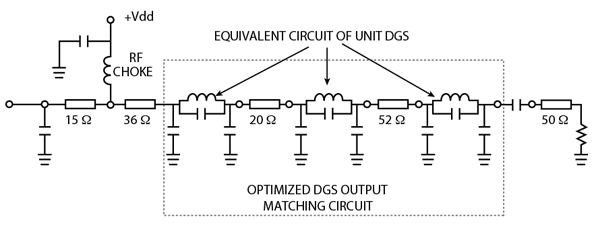
There are two ways to reject the second harmonic with DGS circuits. One is the simple implementation of the DGS circuit in the output transmission line of 50 Ω to have a bandgap at the second harmonic frequency. However, it is difficult to realize the exact 50 Ω -DGS line.8 Another is to have the whole output matching circuit showing a bandgap by itself using DGS circuits. The output circuit includes the parallel LC resonator with parallel-connected capacitors at both ends, which corresponds to the unit DGS section.11,12 The output matching circuit involving DGS circuits is optimized to satisfy the optimum load reflection coefficient,  Lopt, by using this equivalent circuit for the unit DGS. Also, this optimized output matching network suppresses the transmission of harmonics. In the previous design method, the output circuit with DGS, which could provide the optimum load reflection coefficient, was designed by iterative EM-simulations for a DGS. However, this method uses the circuit optimizing procedure for the design of a power amplifier including the DGS circuit, which is represented by its equivalent circuits.
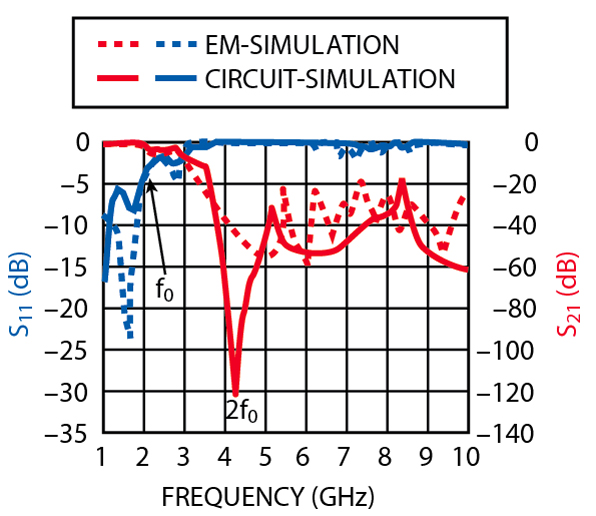
The substrate used for the design and implementation of the output matching circuits is Taconic's TLX-9, which has a dielectric constant of 2.5 and a thickness of 30 mil. At 2.14 GHz and Vds = 27 V, an optimum load impedance of ZL = 11.65-j42.05 Ω was obtained for maximum output power. The implementation of the actual optimized DGS cell used in the amplifier output circuit could be achieved by a simple conformal mapping formula between the dimensions of the original unit cell and the frequency response of its equivalent circuit. To obtain more accurate dimensions of the DGS circuit, iterative 3-D EM simulation is required. Figure 4 shows the comparison of circuit- and EM-simulations for the output matching circuit of the power amplifier. Despite differences in the comparison of the overall simulated performances, the S-parameters are well matched at the fundamental frequency of 2.14 GHz. It is noticeable that by employing the designed output DGS matching circuit for a power amplifier, an excellent rejection for the second harmonic power by 40 dB can be expected.

By using the optimized output DGS matching circuit, a simulation for the output power spectrum with two-tone excitation was performed. Figure 5 shows the predicted fundamental output power and IM product spectral outputs from the amplifier with an input of two tones of equal amplitude at 2.1400 and 2.1405 GHz. The amplitude of the fundamentals for the two-tone simulation was 27 dBm. The predicted results for the designed power amplifier with the DGS matching circuit show fundamental signals of 40.1 dBm and IM3 distortion products of 7.8 dBm.
Design of a Microwave DGS Oscillator
Figure 6 shows a DGS oscillator configuration, which provides an effective parallel feedback path and a frequency-selective circuit by using a DGS. In order to show the validity of the proposed DGS and the oscillator configuration, a 9 GHz DGS oscillator was designed and simulated by using its equivalent circuit.
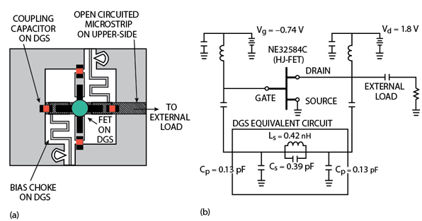
An external lumped element or device mounted on DGS is represented as the parallel-connected element or device with the equivalent circuit of the unit DGS section. Thus, the DGS circuit provides a parallel feedback path to the mounted device on DGS. The equivalent circuit model and the modeling method for a DGS circuit are detailed in a previous paper.12 The effect of an external lumped element on a DGS circuit can be explained by the parallel connection with the equivalent circuit of a DGS.16 The oscillator uses a defected ground structure section as a feedback loop for simultaneously inducing the negative resistance and a passive frequency-selective circuit. The DGS oscillator was designed with a NE32584C GaAs hetero-junction FET in common source configuration for achieving the gate-to-drain feedback. The final design of the DGS oscillator circuit involves the DC chokes by using quarter-wavelength transformers and radial stubs. The harmonic balanced simulation on the designed DGS oscillator shows an estimated fundamental output level of 15 dBm with excellent second harmonic rejection performance.
Implementations and Measurements
Performance of the Fabricated DGS Low Pass Filter
The designed three-section DGS low pass filter was implemented using the DGS cells. The overall length including the 50 Ω microstrip feeding lines is 52 mm. The filter is composed of the two kinds of DGS sections and four interconnecting microstrip lines. Figure 7 shows the comparison between simulations on the designed DGS low pass filter and measurements on the fabricated one. A complete full-wave analysis result on the designed DGS low pass filter is shown together with the S-parameters of the corresponding equivalent-lumped low pass filter model. EM-simulated S-parameters in the passband of the optimized DGS low pass filter are in good agreement with the circuit simulated ones for the optimized equivalent circuit.
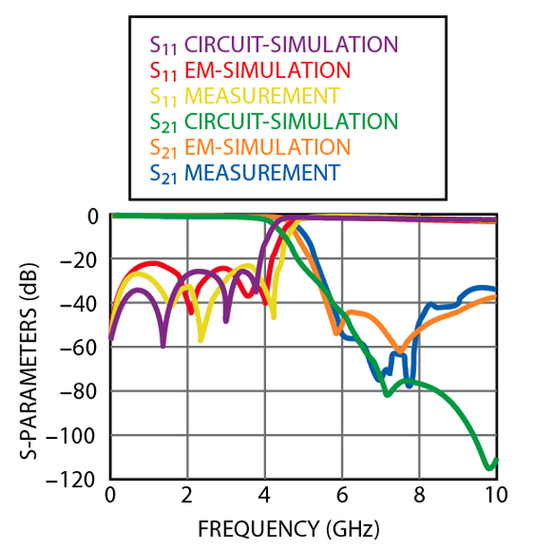
The small deviation of the cutoff frequency performance in the EM-simulation can be attributed to accumulated discontinuity effects at the junction of microstrip lines and DGS cells. However, both simulations demonstrate the optimum performance in the passband and stopband. The return losses are less than -20 dB up to 4 GHz and the second harmonic rejections are greater than 40 dBc in both simulations. The fabricated DGS low pass filter exhibits a minimal insertion loss (better than -0.2 dB) from DC to 4 GHz.
A possible wide stopband exists above this passband, which can be enhanced by cascading several DGS cells in series. The measurement shows good agreement with the simulations on the optimized three-section DGS low pass filter. Finally, since implementation of the proposed DGS low pass filter is based on the optimization on its equivalent circuit, the filter design procedure is greatly simplified.
Fabricated DGS High Power Amplifier's Performance

The performance of the designed output DGS matching circuit, described previously, shows good agreement with that of the optimum load condition. The power amplifier designed with the output DGS matching circuit was expected to show improved efficiency by rejection of the second harmonic. In order to investigate the performance improvement of the power amplifier designed by the proposed method, three kinds of power amplifiers have been fabricated with different types of output matching circuits and their performances compared. Recently, in order to improve the efficiency of a power amplifier, Lim, et al.3 have used an output circuit with DGS in which the cell is designed without consideration of its equivalent circuit. In contrast, the output DGS matching circuit described in this article has been optimized to obtain the load conditions providing the maximum output power and the desirable harmonic rejection to improve the efficiency. The dimensions of the DGS cells used in the previous method were identical, while those of the DGS cells included in the optimized output circuit are different since each cell is optimized, using its equivalent circuit.
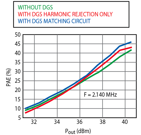
When the fabricated power amplifiers were tested, the two-tone input was excited with a tone spacing of 500 kHz. The measured fundamental output of the power amplifier with output DGS matching circuit was 40.5 dBm with a peak power-added efficiency of 46 percent. A measured IM3 of -33.5 dBc was obtained by using this technique. Figure 8 shows the measured two-tone output spectrum for the power amplifier with the output DGS matching circuit. The power gains of the fabricated power amplifiers were all 13 dB. A 1 W class-A pre-amplifier was used to drive the power amplifiers. The designed output DGS matching circuit provides excellent rejection for the second harmonic power. The second harmonic performance of the power amplifier with the output DGS matching circuit was measured. The measured harmonic spectrum at maximum output power shows that the second harmonic power is -18.17 dBm by using the designed output DGS matching circuit. The improvement in rejection of the second harmonic spectrum was achieved with a 40 dB difference compared with that of a conventional power amplifier. The improvement of 40 dB rejection for the second harmonic power corresponds to that of the designed output DGS matching circuit at 2fo. Also, a comparison of the PAE for the three cases is shown in Figure 9 . It is noticeable that the power amplifier having DGS matching circuit shows more reduction of the second harmonic spectrum than that of a conventional power amplifier without any degradation of fundamental output power performance. Furthermore, an improvement of 30 dB reduction in second harmonic power, compared with the power amplifier having the DGS output circuit only for rejection of second harmonic power, has been achieved by using the presented design method.
Because of the remarkable reduction of the second harmonic output, the resultant PAE of the optimized DGS matching circuit was improved by 2.5 to 6 percent compared with that of other power amplifiers. The fabricated power amplifiers are shown in Figure 10 .

Fabricated Microwave DGS Oscillator's Performance
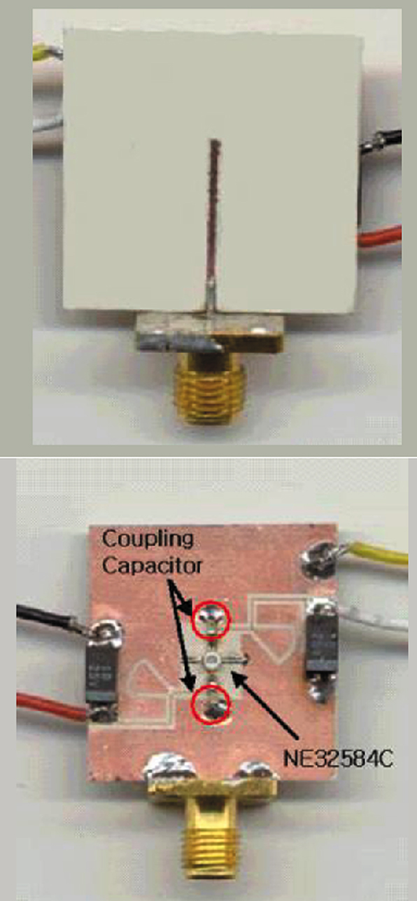
Figure 11 shows the measured output spectrum of the fabricated DGS oscillator. The oscillation frequency ω or of the DGS oscillator is 8.94 GHz, while the resonant frequency ω o of the DGS circuit is near 10.2 GHz. The role of the DGS section in the oscillator presented in this article is to simultaneously achieve a feedback loop and a passive frequency-selective circuit. When the DGS serves as a resonant circuit, the parallel resonant circuit in the equivalent circuit of the DGS is combined with the parallel capacitance, Cp1. This is the reason why the oscillation frequency of the self-resonant oscillator is lower than the resonant frequency of the DGS circuit. The output power of the oscillator is 9 dBm at Vds = 1.8 V and Vgs = -0.7 V. This circuit dissipates 20 mW from a 1.8 V supply. The PAE of the presented oscillator is close to 40 percent. The relatively high output power is due to the choice of the gate-to-drain feedback circuitry. The designed DGS oscillator produces very low harmonic contents. The second harmonic is only -31 dBc below the fundamental frequency. The phase noise at 100 kHz offset from the carrier (fo = 8.94 GHz) is measured to be -87.61 dBc/Hz. The phase noise performance is degraded due to the poor quality factor of the implemented DGS feedback loop. Figure 12 shows photographs of the fabricated DGS oscillator.

Conclusion
In this article, a more accurate equivalent circuit model than the previously reported equivalent circuit of the DGS has been presented. By using parametric relations, the equivalent circuit parameter extraction method for the unit DGS cell has also been derived. In order to demonstrate the usefulness of this method, a harmonic rejection DGS low pass filter was designed with an optimization procedure on the proposed equivalent circuit of the DGS. Both simulations and measurement on the optimized DGS low pass filter have demonstrated the optimum performances in the passband and stopband. Very efficient design methods have been described for a power amplifier and a microwave oscillator that employ the DGS as a part of the circuit. The design technique using an equivalent circuit of a DGS is well applicable to implement an active circuit, suppressing the harmonic generation, with no limits in MIC or MMIC applications.
Acknowledgment
This work was supported by the Korea Foundation under Grant KRF-2001-042-E00041.
References
1. V. Radisic, Y. Qian and T. Itoh, "Broadband Power Amplifier Using Dielectric Photonic Bandgap Structure," IEEE Microwave and Guided Wave Letters , Vol. 8, No. 1, January 1998, pp. 13-14.
2. V. Radisic, Y. Qian, R. Coccioli and T. Itoh, "Novel 2-D Photonic Bandgap Structure for Microstrip Lines," IEEE Microwave and Guided Wave Letters , Vol. 8, No. 2, February 1998, pp. 69-71.
3. J.S. Lim, H.S Kim, J.S. Park, D. Ahn and S. Nam, "A Power Amplifier with Efficiency Improved Using Defected Ground Structure," IEEE Microwave and Wireless Components Letters , Vol. 11, No. 4, April 2001, pp. 170-172.
4. C.S. Kim, J.S. Park, D. Ahn and J.B. Lim, "A Novel One-dimensional Periodic Defected Ground Structure for Planar Circuits," IEEE Microwave and Guided Wave Letters , Vol. 10, No. 4, April 2000, pp. 131-133.
5. J.I. Park, C.S. Kim, J.S. Park, Y. Qian, D. Ahn and T. Itoh, "Modeling of Photonic Bandgap and Its Application for the Low Pass Filter Design," 99 APMC Digest , December 1999, pp. 331-334.
6. Q. Xue, K.M. Shum and C.H. Chan, "Novel 1-D Microstrip PBG Cell," IEEE Microwave and Guided Wave Letters , Vol. 10, No. 10, October 2000, pp. 403-405.
7. D. Ahn, J.S. Park, J. Kim, Y. Qian and T. Itoh, "A Design of the Low Pass Filter Using the Novel Microstrip Defected Ground Structure," IEEE Transactions on Microwave Theory and Techniques , Vol. 49, No. 9, January 2001, pp. 86-93.
8. J.S. Lim, S.W Lee, J.S. Park, D. Ahn and S. Nam, "A 4:1 Unequal Wilkinson Power Divider," IEEE Microwave and Wireless Components Letters , Vol. 11, No. 3, March 2001, pp. 124-126.
9. C.S. Kim, J.S. Lim, J.S. Park, D. Ahn and S. Nam, "A 10 dB Branch Line Coupler Using Defected Ground Structure," Proceedings of the EUMC2000 , Vol. 3, October 2000, pp. 68-71.
10. K.M. Shum, Q. Xue and C.H. Chan, "A Novel Microstrip Ring Hybrid Incorporating a PBG Cell," IEEE Microwave and Wireless Components Letters , Vol. 11, No. 6, June 2001, pp. 258-260.
11. J.S. Park, J.S. Yun and D. Ahn, "A Design of the Novel Coupled Line Bandpass Filter Using Defected Ground Structure with Wide Stopband Performance," IEEE Transactions on Microwave Theory and Techniques , Vol. 50, No. 9, September 2002, pp. 2037-2043.
12. J.S. Park, J.H. Kim, J.H. Lee, S.H. Kim and S.H. Myung, "A Novel Equivalent Circuit and Modeling Method for Defected Ground Structure and Its Application to Optimization of a DGS Low Pass Filter," 2002 IEEE International Microwave Symposium Digest , Vol. 1, June 2002, pp. 417-420.
13. S.C. Cripps, RF Power Amplifier for Wireless Communication , Artech House Inc., Norwood, MA 1999, pp. 88-90.
14. J.L.B. Walker, High Power GaAs FET Amplifiers , Artech House Inc., Norwood, MA 1993, pp. 210-212.
15. S. Mazumder, A. Azizi and F. Gardiol, "Improvement of a Class-C Transistor Power by the Second Harmonic Tuning," IEEE Transactions on Microwave Theory and Techniques , Vol. 27, No. 9, May 1979, pp. 430-433.
16. J.S. Park, C.S Kim, H.T. Kang, G.Y. Kim, K.H. Park and D. Ahn, "A Novel Resonant Microstrip RF Phase Shifter Using Defected Ground Structure," 30th European Microwave Conference Digest , Vol. 2, October 2000, pp. 72-75.
Jun-Seok Park received his BS and MS degrees in electronic engineering and his PhD degree in radio frequency and monolithic microwave and integrated circuits from Kookmin University, Seoul, South Korea, in 1991, 1993 and 1996, respectively. In 1997, he joined the department of electrical engineering at the University of California at Los Angeles, where he was a post-doctoral researcher. From 1998 to 2003, he was an assistant professor in the division of information technology engineering at Soonchunhyang University, Asan, South Korea. He is currently an assistant professor at Kookmin University's school of electrical engineering. His current research involves RF and microwave hybrid module design using low temperature co-fired ceramic (LTCC) techniques and surface acoustic wave devices.