
A line of variable gain amplifiers (VGA) has been introduced for use in transmitter and receiver automatic gain control (AGC) circuits, and as variable gain blocks following low noise amplifier stages in high dynamic range receiver front ends. The new amplifiers integrate high performance amplifiers and attenuators within a single surface-mount package optimized for wireless infrastructure and other telecommunications applications.
The new amplifier series consists of the models VG101 and VG111 integrated VGAs that maintain constant intercept and compression point performance over the entire gain control range. Both amplifiers feature a wide dynamic range of over 30 dB and a 4.3 or better noise figure (NF) at maximum gain. They operate from a single positive bias supply and are matched to 50  over the full attenuation range to ensure proper operation when cascaded with other RF elements such as filters. The combination of gain, NF, attenuation and third-order intercept (IP3) make these devices ideal for base station transmitter and receiver chains that process complex digital modulation formats such as CDMA, GSM, PCS and UMTS. The amplifiers are also well suited for cable, ISM, WLL, WLAN and defense applications. The model VG024 VGA is well suited for temperature compensation circuits with independent gain and slope adjustment. Table 1 lists the key specifications of each of the three models.
|
Table 1 | |||
|
|
VG024 |
VG101 |
VG111 |
|
Frequency (MHz) |
50-2200 |
750-1000 |
1800-2200 |
|
Gain (dB) |
16 |
16 |
14 |
|
Attenuation range (dB) |
18 |
29 |
28 |
|
OIP3 (dBm) |
+40 |
+40 |
+38 |
|
P1dB (dBm) |
+21 |
+21 |
+21 |
|
Noise figure (dB) |
5.5 |
4.1 |
4.1 |
|
Current (mA) |
150 |
150 |
150 |
|
Control Voltage (V) |
0-4.5 |
0-4.5 |
0-4.5 |
|
Bias (V) |
+5 |
+5 |
+5 |
|
Package styles |
SOIC-8 |
28-pin QFN |
28-pin QFN |

VG024
The VG024 amplifier is a high dynamic range VGA in an SOIC-8 package with metal slug on the back side for better thermal operation. The amplifier can be adjusted to operate anywhere in the 50 to 2200 MHz frequency range using several off-chip components. The output third-order intercept point (OIP3) and 1 dB compression point (P1dB) performance is maintained over the entire control range. An inexpensive dual op amp circuit allows the VG024 amplifier to operate as an RF chain temperature-compensation stage that features independent and adjustable offset and slope control, while providing lower losses and larger slopes than can be achieved with thermistor networks or thermal compensation pads. In addition, a single op amp circuit can be used as a voltage variable driver, providing temperature stable voltage variable gain operation. With a simple NPN driver, the VG024 amplifier is ideal for AGC circuits in transmitters and receivers. Figure 1 shows the VG024 VGA's pinout configurations and Figure 2 shows the amplifier's performance as an automatic gain control amplifier.

VG101 and VG111
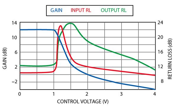
The model VG101 is a high dynamic range attenuator with gain that operates at +5 V with a total current consumption of less than 200 mA. The part is housed in a 6 x 6 mm 28-pin QFN package. Its attenuation range is 30 dB in a typical example drive circuit for a control voltage of +4.5 V and gain control pin current of 15 mA. The VG101 VGA is designed to operate in the 750 to 1000 MHz frequency range, which includes the cellular transmit and receive bands. Both the VG101 and VG111 are very similar, but operate at different frequencies. The large dynamic range for the attenuator and specific operating frequency makes these parts suitable for power control in the RF sections of cellular (VG101) and PCS/UMTS (VG111) base stations, respectively. Other applications include power control for repeaters and in other RF equipment when automatic gain control loops are implemented. Both transmit and receive bands benefit from the low noise figure, large attenuation range and high linearity. Figure 3 shows the pinout diagram for the VG101 and VG111 devices. Figure 4 shows the VG101 VGA's gain and return loss vs. control voltage.
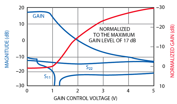
The attenuator is in front of the amplifier in the entire family of VGAs, which gives constant P1dB and OPI3 at all attenuation values. Integrating an attenuator and amplifier into one multi-chip module (MCM) reduces the overall parts count and layout size for an RF attenuator block. The noise figure and loss of the VG101 device is still acceptable because of the low attenuator loss. The VG101 acts like a very good linear amplifier, although increasing the attenuation will contribute directly to increasing the noise figure and IIP3, but not the OPI3 and P1dB. The high OPI3 and P1dB along with the low NF makes placement in an RF chain very flexible, though cascading VG101 and VG111 parts requires careful chain analysis to prevent degradation of the overall noise of the system.
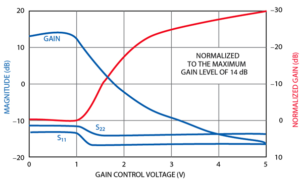
The VG111 VGA is a high dynamic range variable attenuator with gain and similar characteristics to the VG101 unit except the operating frequency range is 1800 to 2200 MHz. The frequency range includes the PCS and UMTS transmit and receive bands. This device also has the attenuator in front of the amplifier. However, the internal matching and amplifiers are different in the VG111 for the PCS/UMTS bands to achieve similar performance as the VG101 in the cellular band.
There is internal amplifier matching for the higher frequency operating band, and there are external components that must be added to the RF circuit. An external 2.2 resistor is added to maintain unconditional stability at all load conditions, and shunt capacitance near the RF input improves the input return loss at higher frequencies. External output shunt capacitors are required to improve the output matching and the best match can be shifted to lower frequencies by increasing the separation of the shunt capacitance and the RF output. Operation of the VG111 is essentially the same as the VG101. Figure 5 shows the VG111 gain and return loss performance.
Conclusion
A new family of variable gain amplifiers has been introduced that will allow design engineers to achieve simpler, more cost-effective systems while offering new levels of performance to wireless equipment. Fully assembled evaluation boards and loose samples are currently available and can be requested from the company's Web site.
WJ Communications, San Jose, CA (800) 951-4401, www.wj.com. Circle No. 303