
A versatile new three-stage buffer amplifier has been introduced that is ideal for use as a receiver front end low noise amplifier, but, as a result of its dual bias configurations, it can also be used as a driver amplifier or LO buffer with good linearity and higher gain. The XB1005 MMIC low noise amplifier uses a 0.15 µm gate length GaAs pseudomorphic high electron mobility transistor (pHEMT) device model technology and operates from 35 to 45 GHz.
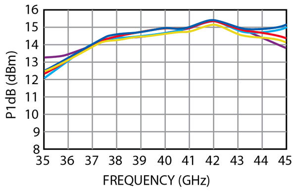
Primarily designed for wireless communications applications, the three-stage device can be operated with all three stages biased in parallel or with independent bias for input and output stages, as required to optimize performance. The MMIC device has a small signal gain of 20 dB with a noise figure of 3 dB across the entire operating band. It features a 14 dBm P1dB at low noise bias, or can provide 18 dBm P1dB with higher gain at a bias setting optimized for driver amplifier applications. As a result, this new device serves as an excellent LNA or buffer amplifier for wireless communications applications such as millimeter-wave point-to-point radio, local multipoint distribution services (LMDS), SATCOM and VSAT applications. In most of these applications the XB1005 amplifier displays excellent low noise characteristics and the linearity is sufficient. However, with higher signal levels the bias can be increased to improve linearity at a small noise figure penalty.
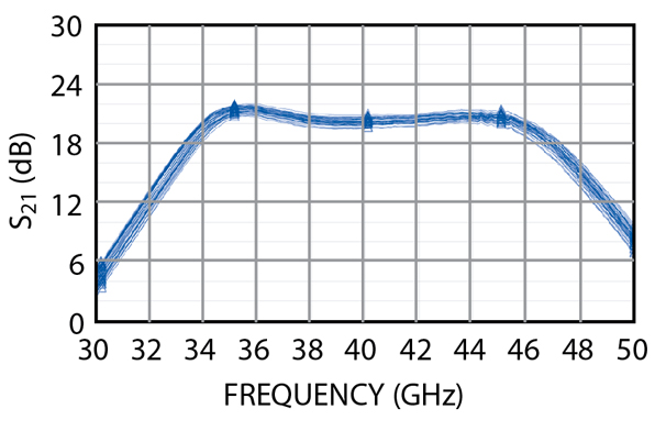
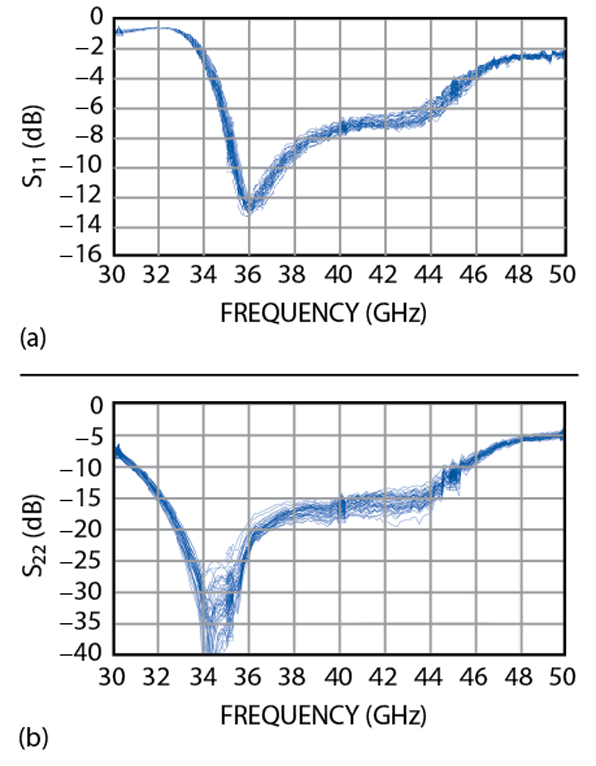
Typical electrical specifications at 25°C over the 35 to 45 GHz frequency range include input (S11) and output (S22) return losses of 8 and 17 dB, respectively, small signal gain (S21) of 20 dB and a gain flatness of ±1 dB. Reverse isolation (S12) is 45 dB and the output third-order intercept point (OIP3) is +24 dBm. Typical supply current at Vd = 3.5 V and Vg = -0.4 V is 50 mA.
Measurements were made on many amplifier samples to demonstrate performance consistency. Figure 1 shows the amplifier's input and output return losses vs. frequency. Figure 2 displays the device's gain characteristics and Figure 3 is a plot of P1dB using typical low noise biasing.
The GaAs pHEMT device is based on electron beam lithography to ensure high repeatability and uniformity. The chip has surface passivation to protect the part and provide a rugged device with backside via holes and gold metallization to allow either a conductive epoxy or a eutectic solder die attach process. The chip measures 0.051" by 0.094" with a 0.004" thickness and has 4 x 4 mil DC bond pads and 4 x 8 mil RF bond pads.
It is recommended that all three stages be biased at Vd = 3.5 VDC and Id = 50 mA, although the best performance will result from separately biasing Vd1 through Vd3 with Id1 = 9 mA, Id2 = 16 mA and Id3 = 25 mA. It is also recommended to use active biasing to keep the currents constant as the RF power and temperature vary. Depending on the supply voltage available and the power dissipation constraints, the bias circuit may be a single transistor or a low power operational amplifier with a low value resistor in series with the drain supply used to sense the current. The gate of the pHEMT is controlled to maintain correct drain current and, thus, the drain voltage. The typical gate voltage required to do this is -0.4 V at low noise bias, and -0.1 V at power bias where the total drain current will be 130 mA at Vd = 4.5 V. In addition, the gate is typically protected with silicon diodes to limit the applied voltage and the voltage is sequenced on to ensure negative gate bias is available before applying the positive drain supply.
Production chips of the XB1005 are 100 percent on-wafer tested for DC, RF and noise figure performance. In addition, there is 100 percent visual inspection to MIL-STD-883 Method 2010. Engineering samples are currently available from stock and production quantities are available two to four weeks ARO.
Mimix Broadband Inc., Houston, TX (281) 988-4600, www.mimixbroadband.com. Circle No. 302