
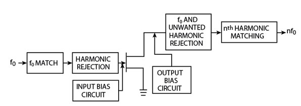
The basic principle of operation of a MESFET multiplier is that the device is biased for a particular conduction angle, based on the harmonic frequency to be generated. A generalized circuit schematic of a MESFET frequency multiplier is shown in Figure 1 .
It can be seen that the generalized circuit appears to be identical to a power amplifier; the only difference is that the output resonator is tuned to the nth harmonic of the fundamental, not the fundamental frequency. Table 1 shows the Fourier components as a function of the conduction angle up to the fifth harmonic.1
FET Multiplier Over Step-recovery Diode Multipliers
Unlike diodes, a MESFET's currents cannot be described by a single equation and thus require a more complex treatment to describe its nonlinear operation. Comparison of MESFET and Schottky diode multipliers is not simple and requires engineering judgment for their specific application. For instance, frequency doublers, built with Schottky-barrier diodes, are lossy (in general > 10 dB), require no tuning elements and can operate over an octave bandwidth, a performance not attainable with MESFETs. On the other hand, if the bandwidth is less than 50 percent, MESFET multipliers have a great advantage over diode multipliers since they can achieve a conversion gain greater than unity (generally kept near unity), depending upon the bandwidth, while maintaining good DC to RF efficiency.
In addition, transistors offer several other advantages compared to diodes, such as isolation between input and output, so that it usually suffices to match the input at the fundamental frequency, and to use only a bandpass filter at the output. They also require much less drive power for generating a significant output power level. Another advantage of MESFETs is that they are an integral part of MMICs where power efficient frequency multipliers can be designed to fit a specific need, saving weight, size and power consumption. These factors are always of great importance in deep space missions or even in terrestrial satellites.
|
Table 1 | ||||||
|
n |
|
I 1 /I p |
I 2 /I p |
I 3 /I p |
I 4 /I p |
I 5 /I p |
|
1 |
360 |
-6.0 |
- |
- |
- |
- |
|
2 |
120 |
-8.4 |
-12.0 |
-17.0 |
-32.0 |
- |
|
3 |
76 |
-12.0 |
-13.2 |
-15.4 |
-18.4 |
-24.0 |
|
4 |
65 |
-13.4 |
-15.4 |
-15.9 |
-18.0 |
-20.0 |
|
5 |
48 |
-14.7 |
-14.9 |
-16.4 |
-18.2 |
-18.4 |
|
pinch-off |
180 |
-6.0 |
-13.2 |
- |
-27.0 |
- |
|
square-wave |
360 |
-3.9 |
- |
-13.5 |
- |
-17.9 |
Nonlinearities involved in MESFETs
There are three nonlinearities that can be utilized to generate harmonic frequencies. The first is the use of the FET gate-source capacitance (Cgs). This nonlinearity has been analyzed as a lossy varactor resulting in harmonic frequency signal levels of -18 to -11 dB below the expected fundamental frequency output power level.2
The second nonlinearity arises from clipping of the Ids waveform. This effect can be induced by biasing the device at 0 V or at pinch-off and causing a half-wave rectified sinusoidal output voltage, which has a theoretical second harmonic level of 7.4 dB below the fundamental frequency output signal.2
The third nonlinearity is due to the nonlinear Vgs-Ids transfer characteristic. FET devices generally exhibit good linearity, and, as a result, do not contribute significantly to multiplier performance.
Simulations using a unilateral FET model2 have shown that the nonlinearity, which is the largest contributor to harmonic generation, is the clipping of the Ids waveform with less significant contributions from Cgs and transfer nonlinearities.
In order to optimize the harmonic generation of the frequency multiplier, attention must be paid to the terminations1-4 that are presented at the device output to the fundamental and nth harmonic frequency signals. Biasing the gate at 0 V (or pinch-off) to create a half-wave rectified output will provide better conversion efficiency if the fundamental frequency signal is terminated in an open circuit and the nth harmonic frequency is extracted with a matched load. This allows a maximum voltage swing of the rectified sinusoidal waveform, which is rich in nth harmonic signal content.
Selection of a MESFET Nonlinear Model
The selection of the proper nonlinear model for the device to be used for simulation purposes plays a very important role in designing a nonlinear circuit accurately. Several appropriate nonlinear MESFET device models such as Statz, Curtice Cubic and TOM can be chosen. The differences between these three models are given below and the user can select an appropriate device model to be used for good accuracy. Also, there may be slight differences in the way a model is implemented in commercial simulators. Although the same model exists in several simulators, each one may use slightly different variable names. For example, most GaAs FET models contain a zero bias gate-source junction capacitance. In PSPICE and MDS, this capacitance is defined as the variable CGS; in LIBRA and COMPACT it is defined as CGSO. These differences require the user to translate model parameters to conform to the syntax of the specific simulator to be used for circuit simulation purposes.
The Statz model is more accurate when the Ids of a device behaves quadratically (square-law approximation) for small values of Vgg - Vp and linearly for large values of Vgg - Vp. The Curtice model is useful when extracting model parameters at a single bias point. Triquint's Own Model (TOM) is more accurate when the square-law approximation does not predict device performance well and when the device drain conductance varies with gate-source bias.
Design of a FET Frequency Multiplier
The design of a frequency multiplier can be initiated by selecting the appropriate gate voltage to control the conduction angle of the FET, keeping in mind the desired harmonic to be generated and the appropriate drain voltage must be selected. The peak reverse voltage across the gate must be taken into account if the MESFET is being biased much below pinch-off voltage (that is if Vgg < Vt). The typical reverse voltage across the gate can be approximated by the expression 2Vgg - Vg,max, a relatively high reverse voltage.
The input bias network typically includes a quarter wavelength high impedance line at the fundamental frequency (fo) that is connected to a bypass capacitor to ground so that no fundamental power leaks into the DC bias. The  /4 high impedance line becomes /2 at the second harmonic (2fo) and acts as a short circuit at the second harmonic frequency.
The gate's short circuit at the second harmonic is less critical; a shorted stub /4 long at the fundamental frequency is adequate to provide the termination. Similarly, a high impedance line of /4 length at the output center frequency (nfo) is used for drain biasing purposes with a parallel bypass capacitor connector to ground. The most important thing that must be addressed is the stability of the circuit. If the circuit is not stable over the full frequency band then it must be stabilized. Any of the stabilization techniques shown in Figure 2 can be used to serve the purpose. Although any of the topologies can be used, care must be taken in employing the best possible configuration according to the stabilizing requirement of the circuit and also to maintain a minimum RF power dissipation.
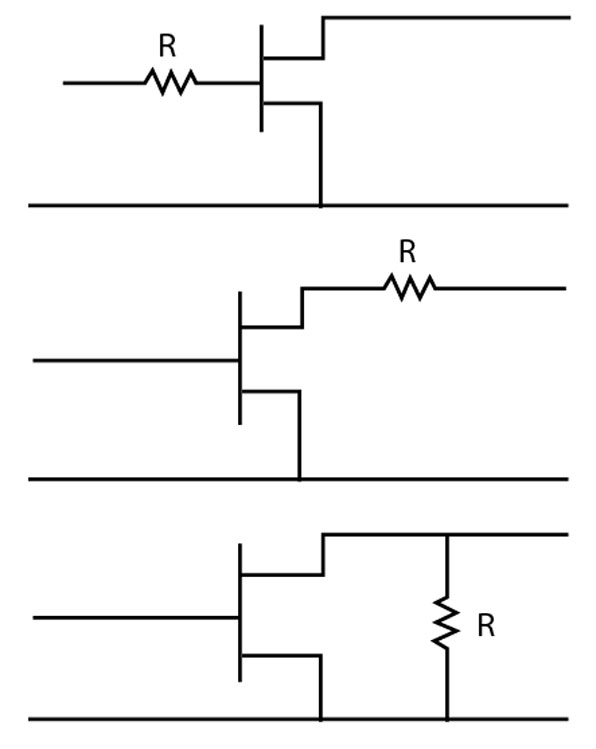
The stability of the circuit is of the utmost importance and, under any circumstances, the stability factor (K) of the circuit must be greater than 1, regardless if some of the conversion gain of the multiplier must be sacrificed. Rejection of the other unwanted harmonics present in the output can be accomplished by a proper open- or short-circuited stub arrangement. These stubs can be open- or short-circuited based on the convenience and size of the circuit. Open-circuited stubs of /4 length at various harmonic frequencies can be connected in shunt to the drain so that it sees a short-circuit load at the unwanted harmonics. The nominal impedance of these shunt stubs may be 50  or some other impedance, depending on circuit requirements.
If the multiplier must operate over a moderate bandwidth, then a bandpass filter can be connected at the output to obtain the best possible flatness over the entire output band. The open- or short-circuited stubs that are used for rejection of unwanted harmonics in the output tend to limit the bandwidth due to their dispersive effect. The choice of the bandpass filter topology depends on the individual's judgment and the system lineup requirements. For example, if the output frequency is high (near Ku-band) then a half-wave filter, consisting of cascaded alternate lines of high and low impedances of length /2 at the desired harmonic frequency, would be a good choice. This filter will provide moderate to high bandwidth without consuming too much space, and if the output frequency occurs in C-band, then a hairpin bandpass filter topology is a good choice to get the required rejection of the harmonics present in the output. In addition, the space occupied will be less than that in the case of a coupled-line bandpass filter topology. If the size requirement of the circuit is not critical then a coupled-line filter can be used in the output.
It remains now to match the input and output sections of the circuit to the 50 source and load terminations. For this purpose, the use of a large signal S-parameter simulation technique, which is available in all RF/microwave nonlinear simulators, is needed. These are power dependent parameters and the required power source must be connected at the input of the device. Any simulator capable of nonlinear simulation can be used for this purpose, such as HP-ADS 1.5 or Microwave Office 2002. The circuit can be re-optimized to obtain better performance for conversion gain, and input and output return losses, using any of the nonlinear simulators available.
MESFET Frequency Multiplier Simulation
The simulated design presented here is for a MESFET frequency tripler using the nonlinear model of an ATF21170 MESFET (available in the HP-ADS 1.5 RF transistor library) for an input frequency of 1500 MHz with a bandwidth of ±50 MHz. The gate and drain biases were fixed, based on the maximum output power at the required third harmonic, after simulating the MESFET for an input power of +4 dBm using the harmonic balance analysis of the HP-ADS 1.5 simulator. The peak reverse voltage across the gate was also taken into account so that it does not cross the maximum specified limit of the MESFET used in the design. The input and output bias networks were then designed by using a high impedance /4 line at the input and output center frequencies, respectively.
The first thing that was established was the stability of the circuit after specifying the gate and drain voltages, and designing the input and output bias network. The linear S-parameter simulation of HP-ADS was used for this purpose. The circuit was not stable over the full frequency range so a resistor was connected in series with the gate (Rs1), and one series resistor (Rs2) and capacitor (Cs1) combination was connected in shunt with the gate. The values of the resistors were adjusted until a stability factor greater than 1 was achieved. Care was taken to keep the value of Rs1 as small as possible so that it did not consume too much of the input power, and the value of Rs2 was kept as large as possible.
A three-section coupled-line bandpass filter centered at 4500 MHz (third harmonic) was connected at the output to provide rejection of the unwanted harmonics in the output. The topology of the bandpass filter was selected as a coupled line because of the available space for the circuit; any other topology will also serve the purpose if the size of the circuit is of major concern.
The large signal S-parameters of the circuit were simulated using HP-ADS 1.5, and the input and output matching networks were designed to match the gate and drain impedances to the 50 source and load terminations. In the present case, single open-circuited stubs on each side (input and output) were sufficient to match the circuit over the entire bandwidth.
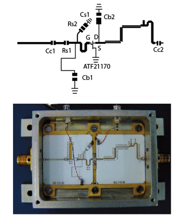
The circuit was re-optimized for better conversion gain, input and output return loss, and passband flatness in the output after completing all the sub-networks design. The complete layout of the frequency tripler circuit and the actual fabricated tripler are shown in Figure 3 . The circuit was designed and fabricated on a 25-mil alumina substrate with a dielectric constant  r = 9.90.
Multiplier Design Formulas
The conduction angle of the FET can be calculated using the expression

The bias voltage which achieves this value of  t is
t is

The optimum load resistance is

RL in a multiplier is usually much greater.
The output power at the nth harmonic, PL,n, is

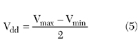
As for a power amplifier, the DC drain bias voltage is halfway between Vmax and Vmin, that is
The input power can be approximated by the expression

and the conversion gain is

The maximum drain-gate voltage is approximately Vmax - Vg,min, so the limitation Vmax - Vg,min < Va, where Va is the drain-gate avalanche voltage, must be respected.
Simulated and Measured Results
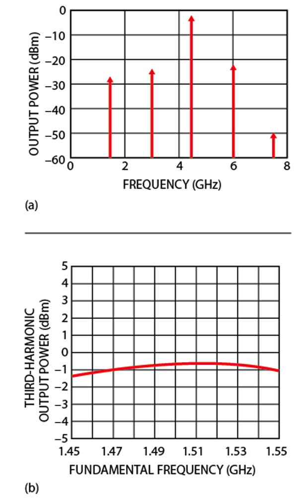
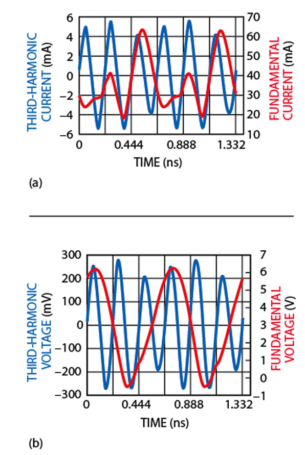
The simulated time domain current and voltage waveforms of the fundamental (red curve) and third harmonic (blue curve) frequencies at the output of the MESFET are shown in Figure 4 . The simulated power spectrum and output passband flatness are shown in Figure 5 . A conversion loss of -1.6 dB, a sideband rejection greater than 20 dB and a passband flatness of 0.7 dB were achieved in the simulation.
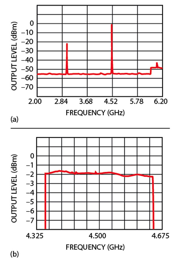
The measured power spectrum and output passband flatness are shown in Figure 6 . A conversion loss of -2 dB, a sideband rejection greater than 20 dB and a passband flatness of 0.6 dB were measured.
Conclusion
A simulation procedure has been demonstrated for the design of a MESFET frequency multiplier, and a frequency tripler was fabricated and its performance verified. The measured results agree closely with the simulation, thus providing a useful engineering tool for the design of nonlinear microwave circuits.
Acknowledgment
The author wishes to thank Shri. S.S. Rana, group director, microwave sensors group, SAC, ISRO, for his constant support and guidance, and Shri. V.H. Bora, head-MSTD, Shri. C.V.N. Rao, sci./engr-SE, microwave integrated circuit fabrication facility and the Mechanical Fabrication Facility for their co-operation extended during the design and development of the described MESFET frequency tripler.
References
1. E. Camargo, Design of FET Frequency Multipliers and Harmonic Oscillators , Artech House Inc., Norwood, MA.
2. A. Gopinath and J.B. Rankin, "Single Gate MESFET Frequency Doublers," IEEE Transactions on Microwave Theory and Techniques , Vol. 30, No. 6, June 1982, pp. 869-875.
3. E. Camargo, R. Soares, R.A. Perichon and M. Goloubkoff, "Sources of Nonlinearity in GaAs MESFET Frequency Multipliers," IEEE International Microwave Symposium Digest , 1983, pp. 343-345.
4. C. Rauscher, "High Frequency Doubler Operation of GaAs Field-effect Transistors," IEEE Transactions on Microwave Theory and Techniques , Vol. 31, No. 6, June 1983, pp. 462-473.
Anurag Bhargava earned his bachelor's degree from North Maharashtra University, Maharashtra, India, and for the last five years has been working in the Space Applications Center, ISRO, Ahmedabad, India.