
PIN diodes have been widely used in a variety of microwave and RF applications, including antenna switches, phase shifters and attenuators. PIN diode attenuators are used extensively in automatic gain control (AGC) and RF leveling applications.
Most PIN diode attenuators control the attenuation characteristics through the forward bias current. This is compatible with the fact that a PIN diode is a current-controlled device and its RF resistance value is set by the forward bias current. Therefore, previous works in this area have concentrated on the current-controlled resistance models of the PIN diode.1-3
Recent PIN diode attenuator studies4 show that the PIN diode attenuator can be controlled by an input bias voltage. The voltage-controlled attenuator with a temperature compensation circuit described by Jang, et al.4 shows excellent linearity and good temperature stability over the operating temperature range.
The design of voltage-controlled PIN diode attenuators requires a PIN diode model, which can describe exactly the relationship between the RF resistance of the PIN diode and its input bias voltage. However, conventional models do not sufficiently express the PIN diode's RF resistance as a function of input voltage, although they can simulate the RF resistance value as a function of the input current. Therefore, the attenuation characteristic of the voltage-controlled PIN diode attenuator designed using conventional models does not agree with the measured results.
This article presents an accurate model that can precisely simulate the attenuation characteristic of voltage-controlled PIN diode attenuators. The model is verified by measurement and by nonlinear simulation using the harmonic balance method. The model will allow RF and microwave designers to better predict the attenuation versus input voltage for a PIN diode attenuator, and can be applied to various circuits using PIN diodes.

Conventional PIN Diode Model
The schematic diagram of a simple shunt-connected PIN diode attenuator is shown in Figure 1 . It comprises a PIN diode, an RF choke inductor and two capacitors for DC blocking. At RF frequencies, the PIN diode essentially appears as a pure linear resistor, Rrf, whose value can be controlled by a DC or a low frequency control signal. At low frequencies, the PIN diode behaves as an ordinary P-N junction diode.
In order to describe the characteristics of the PIN diode, the conventional model uses the series combination of a P-N diode and a variable RF resistor. When the PIN diode is forward biased, its RF equivalent circuit has been generally described as a current-controlled resistor, Rrf, which can be written as1
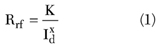
where
Id = DC bias current (mA)
K, x = fitting parameters
The P-N junction diode uses a conventional SPICE model that emulates the DC properties of a PIN diode, and determines the value of Rrf.1-3 The P-N diode is connected in series with an RF resistor to insure the same current flow. The P-N diode parameters within the model are derived from simple DC measurements of the PIN diode.
At the RF frequencies, the P-N diode is effectively RF short-circuited by a large value capacitor, not to influence the RF characteristic. At DC, on the other hand, because the conventional model is expressed as the series combination of the P-N diode model and the RF resistor, Rrf, the variable resistor, Rrf, has an effect on the diode's DC characteristic. Therefore, this RF resistance inevitably deteriorates the DC characteristics.
The input bias voltage Vin and the DC current through the diode Id are given by
V in = V d + R rfI d = V d + R rff(V d) (2)
where
function f(Vd) = I-V characteristic of the diode5


Equations 2 and 3 indicate that the input bias voltage Vin is larger than the diode junction voltage Vd because of the voltage drop caused by Rrf Id. Figure 2 shows the DC I-V characteristic of a PIN diode and the load line which explains the difference between Vin and Vd.
In the case where Rrf = 0, the load line is vertical and the relationship between input voltage and current is the same as the pure I-V characteristic of the diode. In the case where Rrf > 0, the load line is tilted in a counter-clockwise direction, and induces voltage errors. The larger the value of Rrf, the larger this voltage error.
Therefore, the conventional PIN diode model has a problem in including an RF resistor in the DC analysis, and this resistor causes a voltage error in the voltage-controlled PIN diode attenuator simulation. Because the RF resistance value has an effect on DC properties, the conventional models could not be used to produce an accurate attenuation versus voltage characteristic in the simulation of voltage-controlled attenuators.
An Accurate PIN Diode Model

In order to resolve the problems mentioned in the previous section, an accurate PIN diode model, shown in Figure 3 , is suggested. The DC current Id is transformed to the RF part using an ideal current-controlled current source (CCCS) in order to insure the same current flow and remove the effect of the RF resistor on the DC analysis simultaneously. Also, ideal RF choke inductors and bypass capacitors are used to isolate the RF circuit from the DC circuit.
The proposed PIN diode model has perfectly removed the effect of the RF resistor during the DC simulation by way of separating the RF and DC circuits, which makes it a better model for voltage-controlled PIN diode attenuators than the conventional PIN diode model.
Its implementation in a commercial simulator such as Libra™ is shown in Figure 4 . The model parameters are computed using the curve-fitting procedure from Alpha's APD0805 PIN diode data sheets. The APD0805 has low capacitance of 0.05 pF and an 8 mm I-region thickness. This device is selected to exhibit a wide range of resistance versus current and is capable of operating with low distortion as an attenuating element.

In this model, two diodes were used to fit both the DC and RF properties of the PIN diode. The built-in PIN diode model of Libra™ was used to model the behavior of the RF resistance versus DC current according to Equation 1. The P-N junction diode model was used to model the DC voltage-current response. Both diodes were connected in parallel using CCCS to ensure the same current flow and to remove the effect of the RF resistor on the DC analysis. Also, ideal RF choke inductors and bypass capacitors are used to isolate the RF circuit from the DC circuit. The P-N junction diode was effectively RF open-circuited with ideal capacitors C = 1011 pF, while the RF resistance was effectively DC open-circuited with ideal inductors L = 1019 nH to avoid affecting DC performance.
Figure 5 compares the DC voltage-current response simulated by the Libra simulator with the measured values. The DC I-V curve simulated by the proposed model agrees with the experimental result. On the other hand, the simulated I-V curve using the conventional model shows some discrepancy because RF resistance is included in the DC calculation.
Attenuator Design and Results
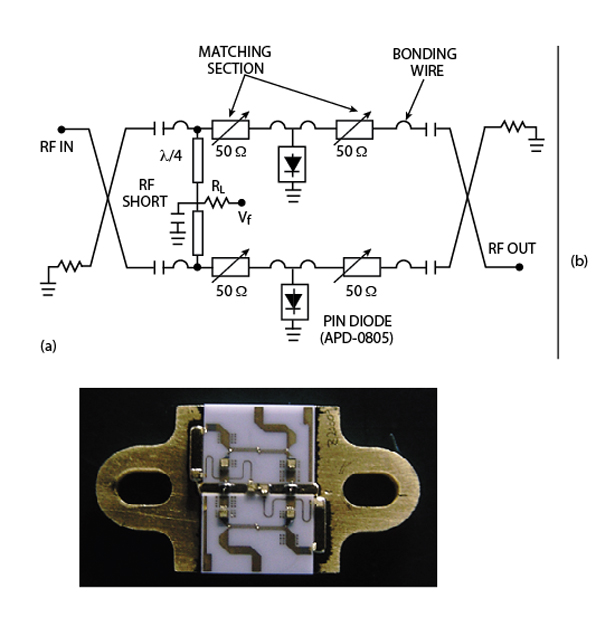
A Ku-band voltage-controlled PIN diode attenuator was designed using the proposed PIN diode model.4 The PIN diode attenuator may take many forms ranging from a simple series- or shunt-mounted diode acting as a lossy reflective attenuator to a more complex structure that maintains a constant matched input impedance across the full dynamic range of the attenuator. In this article, a double hybrid coupled attenuator is chosen, which is capable of providing low input and output SWR and flat frequency response. Figure 6 shows the circuit configuration and photograph of the double hybrid coupled attenuator considered in this study. RL is a load resistor for biasing the attenuator using a voltage source Vf.

The PIN diode device model described in the previous section was linked to the simulator and employed in the design. All circuit-level simulation and layout were done using the Libra harmonic balance simulator. The matching section consists of series microstrip lines that compensate the bonding wire inductance and diode's parasitic capacitance. The PIN diode attenuator was manufactured as a hybrid integrated circuit on a 15-mil thick alumina substrate ( r = 9.8) in a microstrip structure. The diode makes direct contact with RF ground planes and the input bias is applied through quarter-wavelength lines, which appear as a high impedance to the RF signal. The blocking capacitors and bypass capacitors are 68 pF DLI's single-layer capacitors.
Figure 7 shows the attenuation characteristics simulated by the proposed model and the conventional model as a function of input voltage, together with measured values. The attenuation simulated by the proposed model agrees with the measured value. On the other hand, the attenuation simulated by the conventional model is lower than the measured values due to voltage error. From these results it has been demonstrated that the proposed model can simulate the voltage-controlled PIN diode attenuator more accurately than the conventional model.
Conclusion
An accurate model of a PIN diode for voltage-controlled PIN diode attenuators was proposed and verified with experimental data. This model is very effective in designing voltage-controlled PIN diode attenuators, and its implementation in commercial simulators is simple and accurate. Using this model, the attenuation characteristics of a voltage-controlled PIN diode attenuator were successfully simulated. This model resolves the problem in the conventional PIN diode model, and its usefulness in practical applications was confirmed.
References
1. J. Walston, "Spice Circuit Yields Recipes for PIN Diodes," Microwaves and RF , November 1992.
2. G. Hiller, "A CATV Attenuator Using the Single Package SMP1307-027 PIN Diode Array," Application Note, Alpha Industries, 1999.
3. S. Iordanescu, G. Simion, C. Anton and A. Muller, "Broadband Microwave PIN Diode Attenuators," 1998 International Semiconductor Conference Digest , pp. 601-604.
4. B.J. Jang, I.B. Yom and S.P. Lee, "A Voltage-controlled Ku-band PIN Diode Attenuator with a Temperature Compensation Circuit," 32nd European Microwave Conference, September 2002.
5. S.A. Mass, Nonlinear Microwave Circuits , Artech House Inc., Norwood, MA 1988.

Byung-Jun Jang received his BS, MS and PhD degrees in electronic engineering from Yonsei Universitiy, Seoul, Korea, in 1990, 1992 and 1997, respectively. From 1995 to 1999, he worked on CDMA and DECT RF modules for LG Electronics. In 1999, he joined the Electronics and Telecommunications Research Institute (ETRI), Daejon, Korea, where he has been engaged in the research of satellite RF components. His current interests include MMIC and hybrid IC design, and microwave circuit analysis.
In-Bok Yom received his BS degree in electronics engineering from Hanyang University, Korea. Since February 1990, he has been a senior research staff member at the Communications Satellite Development Center of the Electronics and Telecommunications Research Institute (ETRI). He is currently a leader for the satellite RF component team. His research interests include MMIC and satellite payload system design.
Moon-Que Lee received his BS degree in electrical and electronics engineering from the Korea Advanced Institute of Science and Technology (KAIST), Daejon, Korea, in 1992, and his MS and PhD degrees in electronics engineering from Seoul National University, Seoul, Korea, in 1994 and 1999, respectively. Following graduation, he joined the satellite communications system department of the Electronics and Telecommunications Research Institute (ETRI), Daejon, Korea, where he was involved with the development of microwave components and millimeter-wave MMICs for satellite payloads. He is currently an assistant professor in the department of electrical and computer engineering, University of Seoul, Seoul, Korea. His research interests include the analysis, design and optimization of nonlinear microwave circuits.