
Cellular base station receivers work in the presence of high level blockers/interferers while being required to sense weak signals of interest at the antenna. The interferers are usually rejected by filters but only at an intermediate frequency (IF) after the first down conversion. The LNA and mixer preceding the IF filters are required to have high linearity (IP3) and low noise figure (NF).
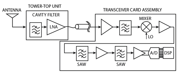
A typical base station receiver featuring simplified block diagrams is shown in Figure 1 . The receiver starts with the antenna featuring a tower-top, very high Q, cavity-tuned filter, and an LNA located close to the antenna. A long coaxial cable connects the received signal to the transceiver, which consists of the cascade of an LNA, a low noise mixer, SAW filters and IF amplifiers, leading to an analog-to-digital converter (ADC). The first mixer performs a conversion down to a typical IF of 70 to 100 MHz (CDMA 800/GSM 900) or 200 to 300 MHz (GSM 1800/GSM1900/UMTS).
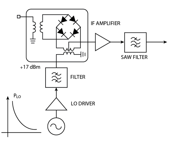
The linearity and noise requirements of the mixer blocks are usually met by passive diode-ring mixers requiring more than 17 dBm drive into the LO port (Figure 2 ). These base station mixers are discrete designs or hybrid modules1 driven by external 50  buffer amplifiers. Therefore, it is possible to filter the local oscillator residual noise before applying it to the mixer. In an IC implementation, care must be taken to specify and design the local oscillator driver noise to meet the system requirements. Filtering can be performed at the input to the chip at a lower oscillator level to limit the noise to kT. The LO phase-noise floor is degraded by the buffer amplifier. In the presence of large blocking signals, the receiver noise increases due to reciprocal mixing of the LO noise with the strong interferers.
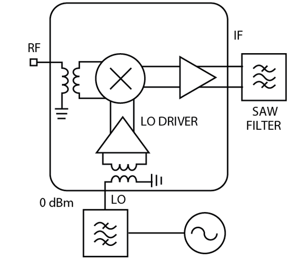
Recently there have been a number of IC mixer designs2,8 targeted to meet base station mixer requirements. These integrated solutions (Figure 3 ) also provide for buffer amplifiers that drive the internal mixer cores, easing the external LO drive requirements to the order of 0 dBm.
While a lot of attention and data is provided for intermodulation (IP3) and noise (NF) of these integrated mixers, the degradation of LO noise caused by the internal buffer amplifiers is not addressed. This article reviews the specification of LO noise in cellular systems and discusses characterization of LO noise in IC base station mixers.
Mixer Noise Model
Thermal noise is the most commonly specified and measured noise in receiver mixers. It describes the noise performance of a mixer that has a 50 matched RF input port with a noise power density of -174 dBm/Hz (kT0). The input-referred thermal noise is determined from the noise figure (10log10F) specification of a mixer.
![]()
where
k = Boltzman's constant (1.381 x 10⁻²³ J/K)
T0 = Absolute temperature (290 K)
F = Noise factor of the mixer
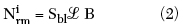
Reciprocal mixing happens in the presence of a strong RF signal at the RF port. This is an additional noise not accounted for during NF measurements. Reciprocally mixed noise  referred to the input can be evaluated at a specific blocker level Sbl. Given an LO noise floor
  into the mixer and a bandwidth B, reciprocally mixed noise at IF is

The phase noise is assumed flat if the interferer frequency offset is a sufficiently large offset from the desired signal. These two noise sources are independent3 and can be summed up, as illustrated in Figure 4 . The signal-to-noise ratio degradation from input to output in the presence of blockers can be expressed as

Specification of LO Noise
Based on the required carrier-to-interference ratio (C/I) at the output of the mixer, the input blocker level (Sbl), the desired signal level (Sdes) and the receiver noise bandwidth (B), the required LO noise performance in dBc/Hz ( ) can be estimated. For GSM base stations, the worst case blocker (Sbl) is -13 dBm, specified for offsets greater than 3 MHz. The desired signal sensitivity is -101 dBm under blocking conditions.5 The bandwidth 'B' for a GSM system is 200 kHz.
= Sdes-Sbl-(C/I)-10log10B (4)
The phase-noise floor works out to -151 dBc/Hz for a GSM base station requiring a C/I ratio of 10. The actual phase noise should be a decibel or so better to account for the degradation due to the front-end thermal noise. The mobile station has a less stringent blocker specification leading to = -138 dBc/Hz.4
Effective Noise Floor of LO Driver
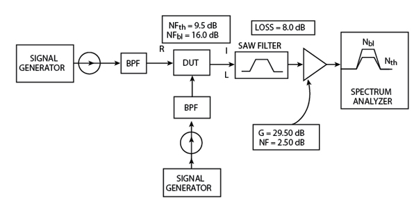
Equations 1 and 2, when substituted into Equation 3, describe the effect of the LO noise floor, (in dBc/Hz), on the signal-to-noise ratio of the receiver. High linearity mixers typically require high LO drive levels and the noise floor of amplifiers can increase by an order of magnitude.6,7 Since reciprocal mixing impresses the LO noise at the IF port as defined by Equation 2, it is possible to measure the noise floor of the LO driver by measurements at the IF. A set-up, shown in Figure 5 , can be used to measure the mixer noise under blocking conditions. The noise floor is measured under no signal and then under blocking conditions. The Nbl is composed of the output thermal noise floor,  , and the output reciprocal mixing noise,
  , altered by the SAW filter and IF amplifier. is determined from small signal noise (F) and gain (G) measurements.
can be separated out of Nbl and the (dBc/Hz) of the integrated LO driver can be computed. Specifying the effective noise floor of integrated circuit mixers helps the system designer estimate the degradation of the signal-to-noise ratio (SNR ) from Equation 3.
Calculation Example
The MAX9993 is an active mixer designed for PCS/DCS/UMTS (1.7 to 2.2 GHz) applications. It has a typical gain of 8.5 dB, a NF of 9.5 dB, an IIP3 = 23.5 dBm and an input P1dB = 13.0 dBm, operating with a local oscillator drive PLO between 0 and 6 dBm.8 The input referred thermal noise,  , is -174 + 9.5 = -164.5 dBm/Hz and the output thermal noise floor, , is -174 + 9.5 + 8.5 = -156 dBm/Hz. The operating frequencies in this example are fIF = 190 MHz, fLO = 1800 MHz and fRF = 1990 MHz. Injecting a 5 dBm blocker offset 25 MHz from fRF (fbl = 2015 MHz) and using a 190 MHz IF filter (SAWTEK 855770) to reject the blocker at 215 MHz, Nbl is measured at -127 dBm/Hz with an Agilent E4404B analyzer. Without the blocker, the noise floor of the set-up is measured at = -134 dBm/Hz. The IF amplifier used in the set-up has a gain of 29.5 dB and a NF of 2.5 dB. The measured agrees with the calculation using the gain and NF of the blocks in the experimental set-up.
The increase in noise floor in the presence of a blocker is attributed to the degradation in signal-to-noise ratio output of the mixer from to Nbl. The noise floor (Nbl) measured by the spectrum analyzer has noise contributions from thermal, reciprocal mixing noise, SAW and IF amplifier. The mixer's effective NF is increased from 9.5 to 16 dB for cascaded block analysis to account for the measured total output noise power. From the composite noise (Nbl), the reciprocally mixed noise can be extracted by using the equations developed in the mixer noise section. The signal-to-noise degradation represented in Equation 3 is 16 dB. Solving for in Equation 3 results in

The input-referred reciprocal mixing noise = 15 -174 dBm/Hz = -159 dBm/Hz. Since a 5 dBm blocker is used, is -164 dBc/Hz. This is well below the GSM requirement of -151 dBc/Hz.
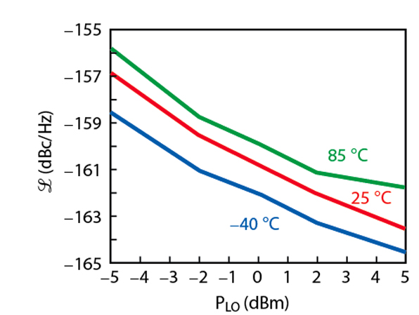
The LO noise defined as a signal-to-noise ratio (dBc/Hz) varies with the LO drive as the drive signal is limited by the LO buffers. This is illustrated in a second example.
The MAX9982 device is a cellular CDMA/GSM band (825 to 915 MHz) high linearity mixer with an input IP3 > 26 dBm, a gain of 3.0 dB and a NF = 11 dB. This mixer is capable of operating with an LO drive ranging from -5 to +5 dBm. Most of the specifications are invariant with the drive signal.8 Figure 6 shows a plot of (dBc/Hz) as a function of the drive level. The set-up used for this measurement is identical to the previous one. An 86.6 MHz GSM IF filter from SAWTEK (854823) is used to attenuate the blocker signal at the IF (5 dBm at the device under test).
Conclusion
The role of the local oscillator buffer amplifier noise in a base station IC mixer design specification has been discussed in this article. Using a simple noise model, the reciprocal mixing component can be extracted from the total noise under blocking conditions. The LO noise of the internal buffer amplifier of two integrated circuit base station mixers has been characterized by measurement of the total output noise under blocking conditions. This data can be used to compute the loss of receiver sensitivity under blocking conditions.
Acknowledgments
The authors acknowledge the help of Jean-Marc Mourant, RF design director, John Newton, executive director and Ted Tewksbury, managing director of the High Speed Signal Processing Business Unit, Maxim Integrated Products.
References
1. Frequency Mixers Level 17. Available at www.minicircuits.com.
2. H. Wohlmuth and W. Simburger, "A High IP3 RF Receiver Chip Set for Mobile Radio Base Stations Up to 2 GHz," IEEE Journal of Solid State Circuits, July 2001.
3. H.J. Yoo and J.H. Kim, "The Receiver Noise Equation: A Method for System Level Design of an RF Receiver," Microwave Journal, Vol. 45, No. 8, August 2002, pp. 20-34.
4. E. Ngompe, "Computing the LO Noise Requirements in a GSM Receiver," Applied Microwave and Wireless, pp. 54-58.
5. Draft GSM 05.05 V8.1.0., European Telecommunications Standard Institute, November 1999, p. 29.
6. J. Lin, et al., ''A Silicon MMIC Active Balun/Buffer Amplifier with High Linearity and Low Residual Phase Noise," 2000 IEEE MTT Symposium Digest, pp. 1289-1292.
7. R.G. Meyer and A.K. Wong, "Blocking and Desensitization in RF Amplifiers," IEEE Journal of Solid State Circuits, August 1995.
8. MAXIM Integrated Products, MAX9981/MAX9982, MAX9993. Available at www.maxim-ic.com.
Kathiravan Krishnamurthi received his BE in electronics and communications engineering from Regional Engineering College, Tiruchy, Tamil Nadu, India, in 1987, his MS degree in electrical engineering from the University of Saskatchewan, Saskatoon, Canada, in 1990, and his PhD degree in electronics from Carleton University, Ottawa, Canada, in 1995. From 1987 to 1995, he pursued graduate research and published several journal articles in the area of high power PSK modulators, GaAs and InP-based heterostructure varactor devices and frequency triplers. He worked for Nortel Networks from 1995 to 1999 designing CDMA base station transceivers, and in 1999 joined IBM Microelectronics to work on SiGe-based ICs. Since July 2000, he has worked for Maxim Integrated Products, Chelmsford, MA, where he is a senior member of the technical staff responsible for designing high performance base station ICs.
Stephen P. Jurgiel received his BSEE from the University of Lowell, Lowell, MA, in 1985. From 1985 to 1993, he worked at M/A-COM in the development of broadband modules and commercial receivers. From 1993 to 1999, he worked at SierraCom as a senior engineer in the development of point-to-point radios and VSAT equipment. He worked for IBM Microelectronics group from 1999 to 2000 as a systems engineer in the development of highly integrated RFICs for handsets. Since 2000, he has worked for Maxim Integrated Products, Chelmsford, MA, where he is a principal member of the technical staff responsible for the design, development and customer support for high performance base station ICs.