

For the third-generation (3G) mobile radio standards, a very high linearity transmitter that can support high crest factor signals is necessary. High linearity and high efficiency are critical issues in amplifier design.
In fact, as the power amplifier operates close to the saturation region where both high efficiency and high output power are achieved, the degradation in linearity becomes significant. A compromise between power, efficiency and linearity must be considered.
Otherwise, a linearization technique to decrease the nonlinearity of the power amplifier is the only solution. Various linearization methods, such as feedforward, negative-feedback, predistortion, linear amplification with nonlinear components (LINC), combined analog locked loop universal modulator (CALLUM), envelope elimination and restoration (EER), and so forth, have been reported.1

Among the numerous amplifier linearization techniques, feedforward linearization has been extensively used in base station amplifiers because of its intrinsic advantages in providing high linearity over a wide frequency band and tighter specifications of nonlinearity in base station transmitters than in mobile station transmitters. Since the linearizing parameters change dramatically due to varying operating conditions such as temperature, input power level and supply voltage, an adaptive control circuitry is essential in feedforward linearizers. Several adaptive control approaches have been proposed. The fixed pilot tone method,2 the pilot tone hopping method,3 the gradient method,4,5 and the intentional signal perturbation method6 have been reported.
In this article, an analog-controlled adaptive feedforward amplifier linearizing method to reduce signal distortion is derived. This method adjusts the circuit parameters adaptively for varying operating conditions. The feedforward linearizer consists of a main signal cancellation loop and a distortion signal cancellation loop. In the main signal cancellation loop, the magnitudes of two subtracter input path signals and their relative phases to the input signal of the feedforward amplifier are compared and controlled so that the main signal can be cancelled at the output port of the subtracter. In the distortion signal cancellation loop, the distortion signals at the subtracter output port are controlled continuously to have constant gain and phase so that the distortion signals are cancelled at the amplifier output port.
Architecture and Operating Principles
The fundamental structure of a feedforward amplifier consists of two signal cancellation loops. Based on the assumption that the amplifier output signals are the sum of the amplified input signal and distortion signals, the amplified input signal is cancelled in the main carrier cancellation loop, which leaves only the distorted signals. In the distortion signal cancellation loop, the distorted signals are amplified and cancelled at the output port of the feedforward amplifier, which only leaves the amplified input signal as the final output signal. Though theoretically the feedforward structure can provide a completely distortion-free output signal, the actual achievable output signal is dependent on the imbalances in the amplitude, phase and delay time of each signal path in the loops.

Figure 1 shows the schematic diagram of the proposed analog-controlled feedforward amplifier. The input signal is applied to a directional coupler, one output of which is connected to the main amplifier through a variable attenuator (A1) and a variable phase shifter ( 1). Some of the amplified input signal and the generated distortion signals at the output of the main amplifier are extracted and connected to the signal subtracter. Another portion of the input signal is also connected to the subtracter after passing through a delay line. The two inputs of the subtracter are connected to an RF switch (RF SW1) via two directional couplers. The RF switch is controlled by a clock and connects one of its two inputs to a divider (D1). One of the divider's output signals is converted to a signal voltage by a detector (DET1). This voltage is connected to one port of a magnitude comparator (MC). In this way, the magnitude of the two signals entering the subtracter can be compared, and the magnitude comparator supplies a voltage VA1 to the variable attenuator so that the magnitude of the two signals entering the subtracter are matched. The magnitude comparator consists of an inverting amplifier and an integrator that can be realized with operational amplifiers.

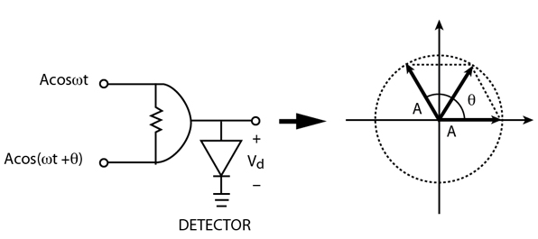
The other output signal of divider (D1) is connected to the RF port of an IQ demodulator, whereas a part of input signal is connected to the LO port of the IQ demodulator. Because the frequencies at the LO and RF ports in the IQ demodulator are the same, the outputs of the IQ demodulator are in-phase and quadrature-phase direct voltages that represent the relative phase data between the LO and RF signals. With the proper connection path through the RF switch (RF SW1), the phase data of two signal paths to the subtracter can be obtained. The phase comparator (PC) consists of two-magnitude comparators and furnishes a voltage (V 1 ) to the variable phase shifter ( 1) so that the phase of two signal paths to the subtracter are out-of-phase. Figure 2 shows the schematic of a manufactured IQ demodulator. Usually, the phase of a variable attenuator changes as the attenuation level is changed. For this application, however, the phase variation of the attenuator used is minimized. The attenuator uses a PIN diode and an external open stub transmission line to compensate for its internal parasitic components causing phase changes. For a good reflection coefficient, a reflection-type attenuator is adopted.7

Direct frequency spectrum comparison is possible in the main signal cancellation loop because the signals in the two paths have a similar frequency spectrum, although frequency spectrum comparison is very difficult in the distortion cancellation loop because the frequency spectrum of the signals in the two paths are dissimilar. The signals at the output port of the main time delay circuit are the sum of the amplified input signal and distortion signals, but the signals that pass through the subtracter are just distortion signals. So a direct comparison of the two signals in the distortion cancellation loop cannot be used to cancel the distortion signals. But if the signals in the two paths can maintain constant gain and phase in spite of changing operating conditions so that the same level and out-of phase of distortion signals in the two paths are obtained, the distortion signals can be cancelled. Usually the insertion loss characteristic of a delay line is almost constant, but its phase characteristics change with the operating temperature. By using a variable phase shifter ( 3), controlled by a temperature sensor, the phase of the distortion signal can be made to track out-of-phase with the distortion signals of the main path.
The signal at the output port of the subtracter goes through a divider (D2), a variable attenuator (A2), a variable phase shifter ( 2) and an error amplifier. Most of the amplified distortion signal is connected to the output combiner, and a portion of it is connected to the divider (D4), which goes through an automatic level controller (ALC) and an RF switch (RF SW2). The signal from the subtracter is also connected to another automatic level controller and RF switch (RF SW2). The output signals of the RF switch are converted to signal voltages and the signal voltages are compared in a magnitude comparator. When the gain of the error amplifier changes according to the operating conditions, the magnitude controller (MC) controls the attenuation voltage (VA2) of the attenuator (A2) so that a constant gain is maintained.8

Some of the output signals in the subtracter and the error amplifier are passed through automatic level controllers (ALC), combined with a combiner and converted to detection voltages in a detector (DET3). Since the ALC consists of a low phase shifting attenuator and a detector, there is little phase variation in the automatic level control process. The level of the combined signals differs by the phase difference between input signals. Hence, the detection voltage of the combined signal is also different. That is, the detection voltage shows the phase difference between the input and output signals. The magnitude comparator compares this detection voltage with a fixed voltage and supplies a control voltage (V2) to the variable phase shifter ( 2). Then the phase of this amplified distortion path can be maintained constant. Figure 3 shows the idea behind the phase controller.
Experiments and Results
To validate the proposed linearizing method, a prototype analog-controlled adaptive feedforward amplifier operated in the IMT-2000 base station transmitting band was fabricated. The main amplifier chain consists of an ERA-5SM amplifier from Mini-Circuits and an MHL-21336 amplifier from Motorola. The gain and P1dB of the main amplifier are 47±0.1 dB and 34.7 dBm, respectively. The chain of the error amplifier consists of two ERA-5SM devices and an MHL-21336, and its gain is 53±0.1 dB. The low phase shift, variable attenuator is realized as a reflection-type with ±0.15° phase shift variation over a 20 dB attenuation. The PIN diode used is HSMP-4810 from HP. The variable phase shifter is realized as a reflection-type for good reflection characteristic and a 55° phase variation is obtained for a 12 V change. The varactor diode used is a 1T362 from Sony.

The three-carrier IS-95 CDMA base station transmitting signal is used as the input signal with a center frequency of 2140 MHz. Figure 4 shows a 34.1 dB main signal cancellation when the average output power level is 18.3 dBm. A main signal cancellation of 19.4 to 34.1 dB is achieved for an average output power range of 15.2 to 25.6 dBm, as shown in Figure 5 . With the proposed method, a 20.8 dB improvement in ACPR is obtained, and Figure 6 shows the ACPR improvement results when the average output power level is 23.4 dBm. An ACPR improvement between 6 and 20.8 dB is achieved for a power output varying from 15.2 to 25.6 dBm, as shown in Figure 7 . When the operating frequency changed from 2130 to 2150 MHz, similar main signal cancellation and ACPR improvement characteristics were obtained.
The fabricated feedforward amplifier was also tested with IS-95 CDMA 3 carriers with 1.25 MHz spacing and a center frequency of 2.14 GHz. The ACPR improvement is 21 dB at an average power output of 24.6 dBm, as shown in Figure 8 . Over the output power range, the ACPR improvement results vary from 5.6 to 21.4 dB, as shown in Figure 9 .
This linearizing method can be useful in high power amplifier applications. The output signals at the output ports of the main amplifier and the error amplifier are coupled with a 10 dB coupler. If the coupling is decreased, the proposed linearizing method can be used in high power amplifier operation.
Conclusion
A new analog-controlled adaptive feedforward amplifier linearizer has been presented. In the main carrier cancellation loop, the magnitude and phase of the signal in the two paths to the subtracter are compared and controlled individually for main signal cancellation. In the distortion signal cancellation loop, the gain and phase of each path is controlled to be constant, so that the two distortion signals are maintained at the same level and out-of-phase. The proposed adaptive linearization method was successfully operated, while varying the operating conditions.

References
1. P.B. Kennington, High Linearity RF Amplifier Design , Artech House Inc., Norwood, MA 2000.
2. D.L. Tatterstall, "Feedforward Amplifer Network with Frequency Swept Pilot Tone," US Patent No. 5,130,663, 1992.
3. M.G. Choi, Y.C. Jeong and I.H. Park, "Method and Apparatus for Amplifying Feedforward Linear Power Using Pilot Tone Hopping," US Patent No.,081,156, 2000.
4. R.H. Bauman, "Adaptive Feedforward System," US Patent No. 4,389,618, 1983.
5. J.K. Cavers, "Adaptation Behavior of a Feedforward Amplifier Linearizer," IEEE Transactions Vehicular Technology , Vol. 44, No. 1, 1995, pp. 31-40.
6. M.G. Overmann and J.F. Long, "Feedforward Distortion Minimization Circuit," US Patent No. 5,077,532, 1991.
7. W.T. Kang, I.S. Chang and M.S. Kang, "Reflection-type Low Phase Shift Attenuator," IEEE Transactions on Microwave Theory and Techniques , Vol. 46, No., pp. 1019-1021.
8. I.H. Kang, I.K. Chang, Y.C. Jeong and S.W. Yun, "The Design of Automatic Gain and Phase Controlled Amplifier," APMC Digest , 1995, pp. 18-21.
Yong-Chae Jeong received his BSEE and MSEE degrees in electronics engineering from Sogang University, Seoul, South Korea, in 1989 and 1991, respectively. From 1991 to 1998, he worked as a senior engineer for Samsung Electronics. In 1996, he received his PhD in electronics engineering from Sogang University. In 1998, he joined the Division of Electronics and Information Engineering, and the Institute of Information and Communication at Chonbuk National University, Chonju, South Korea. He is now an associate professor, and is currently teaching and conducting research in the area of microwave devices and base station amplifiers.
Young-Jean Song received his BS and MS degrees from Chonbuk National University, Chonju, South Korea, in 2001 and 2003, respectively. His research interests include linear power amplifiers.
In-Ju Oh received her BS and MS degrees from Chonbuk National University, Chonju, South Korea, in 1995 and 2002, respectively. She is currently employed as an engineer at Telson Electronics, where she works in the area of RF systems for CDMA mobile phones. She is interested in the design of power amplifiers.
Chul-Dong Kim received his BS degree in electronic engineering from Seoul National University, Seoul, South Korea, in 1971, and received his PhD degree in electronic engineering from the University of Wisconsin in 1985. He is the president and CEO of Sewon Teletech Inc., a company that specializes in RF power amplifiers.