
As this article is written, it is estimated that 90 to 98 percent of first-level IC interconnects are made using wire bonding technologies. The remaining connections are primarily bump, or flip-chip connections. This ratio is expected to remain the same for the foreseeable future. In general, it will be low input/output (I/O) applications (like memory devices) that will continue to be wire bonded, while higher I/O applications (logic devices) will require bump connections.1
For discussion purposes, wire bonding with 1 mil diameter gold wire will be assumed. Gold wire bonding of this type has been a flexible and reliable interconnect solution since its development nearly 50 years ago. But the demand for smaller packaging, faster performance, longer battery life and higher reliability has driven designers to look at ball bump connections.
The move toward bump connections is driven by many factors, three of which - the need for smaller packaging, improved electrical performance and the demands of high frequency applications - will be discussed in this article.
Smaller Packaging

One needs only look at the evolution of the cellular telephone to understand how packaging has shrunk over the years. The first cellular phones were so large that the bulk of the unit was mounted in the trunk of the car and only a handset was hard-wired into the passenger compartment. Today, phones are carried in a pocket or clipped on a belt. Yet users still complain that they are too big and bulky. Consumers continue to require smaller and smaller units. These demands eventually translate into more efficient designs in the packaging. By using a flip-chip interconnect process the IC can be electrically connected in a more compact fashion. Figure 1 shows a comparison between a wire connection and a flip-chip bump connection. The entire die and interconnect is essentially reduced to the die size plus the bump height. A switch to bump connections can contribute to a 30 percent or larger reduction in the final package size.
Improved Electrical Performance
One of the obvious benefits of the bump interconnect solution is the reduced interconnect length. A typical wire connection might be 30 mils long. A typical bump connection by comparison might be only 2 mils long. For comparison purposes, it can be assumed that this bump has a diameter of 4 mils. This shorter interconnect translates into a lower inductance through the connection path, and with that, reduced signal loss. According to Riley,2 "Eliminating bond wires reduces the delaying inductance and capacitance of the connection by a factor of 10, and shortens the path by a factor of 25 to 100. The result is high speed off-chip interconnection." When compared to a wire connection, the lower inductance of a bump connection will translate into reduced losses and lower power requirements.
Another driver in the need for bump connections is the demand for higher frequency applications. With increased end-user demands for higher data rates, operating frequencies are being pushed to new highs. At some point, the limitation of the wire interconnect will force a redesign to incorporate a bump or flip-chip connection. In general, that threshold is believed to exist for applications that will operate at speeds somewhere between 20 and 50 Gigabits per second.
The Solder Bump Solution
Flip-chip or bump connections are largely made today with a lead-based solder, lead-tin (Pb-Sn) being the most common. The most famous of these solder bump processes is IBM's C4 (Controlled Collapse Chip Connection) process. Variations of this process are in wide use in the flip-chip world. It is estimated that solder reflow is used as a solution in 80 to 90 percent of the total flip-chip market. The remaining 10 to 20 percent of bump connections are achieved using a variety of other methods. In addition to the gold bump solution, other alternatives include a conductive epoxy bump, copper bumps, column-shaped bumps and even spring-type connections. The focus of this discussion is on the gold bump solution.
The Challenges with Solder Bumps
Solder bumps have been used extensively for years with extremely high reliability. However, some of the challenges associated with the solder bump connection have led some process engineers to look at other bump solutions. To begin this discussion, some process characteristics of both the solder and gold bump solutions are compared.
The solder bumping process is accomplished in a foundry-like processing facility. Bumps can be applied through screening, evaporation or electroplating. There are a number of wafer bumping service providers that will accept wafers and process them through their bumping facilities. Wafers are the input to the process and solder-bumped wafers are the output. Note that this is an offline process, involving the transfer of wafers from one facility to another. Any process that involves handling has the potential to have a detrimental effect on process yield.
Note that solder bumping takes place at the wafer level and not the single die level. Stated another way, solder bump deposition is designed around a wafer scale and is not well suited for situations where bumping an individual die is required. Die level bumping is particularly attractive to R&D, process development and small-volume manufacturing processes.
Lead-free Future
Lead-free initiatives are forcing manufacturers to turn away from the comforts of the well-defined lead-tin (Pb-Sn) solder solution. In anticipation of lead-free regulations, fewer and fewer processes can be expected to be developed that will depend on lead-based solders. While lead-free solders are available today, the solder solution has already earned a tarnished reputation. Manufacturers are seeking solder-free packaging solutions.
Bond Pad Metallization and Gold Pad Dissolution
Silicon-based die typically have aluminum coated bond pads where the interconnect takes place. The solder process was developed and optimized around this metallurgy and the solder solution continues to work well for these designs. But recent developments in the fabrication process have resulted in new die material compounds. The latest die materials include GaAs and InP, which typically use gold for the bond pad material. Gold and solder are not as compatible as the traditional aluminum and solder solution. The phenomenon called goldpad dissolution, which refers to the detrimental effects of the gold-solder interconnect over the life of the application, is the most notable.
Conductivity
Gold's conductivity offers perhaps its strongest advantage over solder. A comparison of the properties of the two materials shows that lead (and its alloys) has an electrical resistivity of 22 µΩ-cm, while gold is 2.19. Gold offers an order of magnitude better electrical conductivity.
There are several other challenges to the solder solution including under bump metallization (UBM) and the fluxing/cleaning requirements. Details on these topics will not be covered since it is not the focus of this article. Instead the discussion will be on gold bumping and the connection process.
How Gold Bumps Are Made
Ball bumps can be made with many of the commercially available ball wire bonders that are on the market. In fact, gold ball bumping is truly an evolution of the 50-year-old wire bonding process. A brief look at the wire process shows how the gold bump is created.

Figure 2 shows a typical wire connection between an IC and a lower surface. In this process, a gold ball is forced down and thermo-sonically bonded to a die bond pad to form the first connection in a wire bond. With the ball connected, the wire is then fed out and attached to a second surface to complete the connection. The ball bumping process is a variation of this wire bonding operation. In the ball bumping process, the wire is snapped off after the ball is initially connected to the die. The dashed line indicates the location where the wire process would be terminated to make a ball.

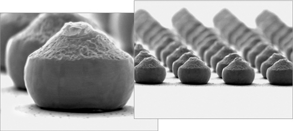
The resulting gold bump (also know as a stud) is firmly connected to the first surface. Figure 3 shows a die that has been "bumped." If subjected to a sideways shear force, these 4 mil diameter bumps can typically withstand up to 50 grams of force before the bond fails. Because of the maturity of the wire bonding process, the reliability of these bump connections is well established and documented.
Coining
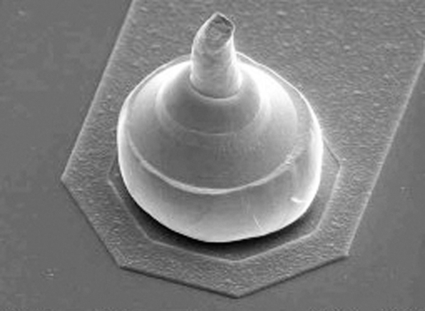
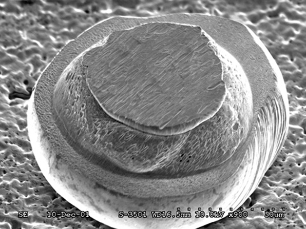
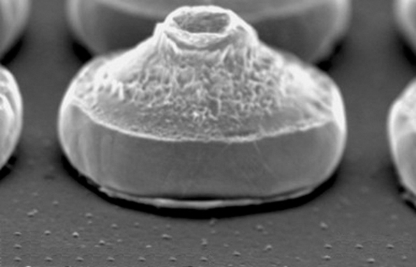
Figure 4 shows the typical shape of a ball bump that has been created by a wire bonder. Note the piece of wire or "tail" on the top of the ball. This peak is a common feature in gold bumps because of the fact that the wire is pulled until it snaps to terminate the ball. As will be discussed in the next section, this tail is not suitable for some flip-chip processes. A process step know as "coining" has been used to flatten the tail and create a flat, round top to the ball, as shown in Figure 5. Coining refers to an application of force that will "smash" the tail into a smooth, flat surface. The diameter of this "plateau" is an important process characteristic as it helps define the area of the gold ball that will contact the second surface. This defines the conduction path.
Bump, Flip and Attach
If the flip-chip process is greatly simplified, we can break it down into three steps: bump, flip and attach. The first step involves the placement of gold bumps on the die, or the first surface. The second step, the flip, will not be discussed. The third step involves the accurate placement and connection to the second surface (the substrate or the package).
Attaching the Flipped Chip
There are four leading alternatives for making a second surface connection. The alternatives are non-conductive epoxy, conductive epoxy, thermo-compression and thermo-sonic compression.
The Non-conductive Epoxy Process

As illustrated in Figure 6, this approach calls for an adhesive material to fill the void between the die and the package, and around the gold bumps. This adhesive, or epoxy, will shrink as it cures and provide the force needed to hold the die and the package together. The connection is made on the second surface with a physical metal-to-metal contact between the gold ball and opposing bond pad on the package. In this case, the ball typically has a coined shape to maximize the surface area in contact.
It is common in this process to use an anisotropic conductive adhesive (ACA). This refers to a particular type of adhesive that becomes conductive only in the Z-direction or, more precisely, in the direction that it is being compressed. The compressed adhesive is that which is trapped between the bump and the package. When this is compressed, conductive particles inside the epoxy align themselves and create a conductive path between the die and the package. Note that there is no conductive path in the X and Y direction, which would, of course, create a shorting path between the bumps.
Conductive Epoxy
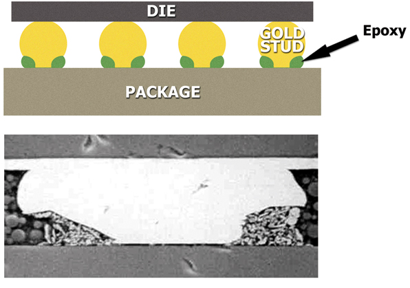
The conductive epoxy solution calls for the application of a small dot of conductive epoxy to the top of each gold stud. As a variation of this solution, the epoxy can be placed on the opposing pad in the package. In either case, the dot of epoxy will provide the "glue" to hold the two surfaces together and complete the electrical path. Figure 7 shows a cross section of a gold bump that has been flipped and connected using the conductive epoxy solution. The conductive epoxy can be seen immediately around and underneath the bump. An underfill material surrounds both the ball and the conductive epoxy. The challenge to this process is in the application of the epoxy in significantly small quantities. Gold bump sizes today range from 2 to 4 mils in diameter. Placing an equal size dot of epoxy can be challenging due to viscosity and dispensing equipment limitations. Solutions available today include positive-displacement dispensers, screening, pin transfer, daubing and gang daubing. The need for smaller epoxy dispensing must be addressed since ball sizes and pitch requirements (distance from ball center to ball center) will decrease over time.
Thermo-compression

In this technique, there are no adhesives used to join the die and the package. Instead, heat and force are applied to the die in a process called "thermo-compression bonding" (see Figure 8). The bumps are forced against their opposing pads and a second metallic bond is formed where the bump comes into contact with the package metallization. In this case, a second bond is created which is similar to the first bond created by the ball bonder. Stated another way, the top and the bottom connection of the ball will be nearly identical, a metal-to-metal connection. This technique typically requires the use of heat as high as 350° to 400°C, and forces of up to 100 g/bump.
The negative side to this process is the fact that the die is subject to high force and temperature. Dies that are thinner, brittle or intolerant of this high heat may not be suitable for attaching using this method. One way to reduce the heat and force requirements is to add an element of ultrasonic vibration and use the thermo-sonic compression solution discussed next.
Thermo-sonic Compression

This process is nearly identical to the thermo-compression solution with the exception that an ultrasonic transducer is used to induce another form of energy to the bonding process (see Figure 9). In this way, the heat and temperature requirements are somewhat reduced.
A frequently asked question is, "Will the application of ultrasonics affect the final placement accuracy of the die?" The actual excursion distance of the vibrated die is measured in micro-inches of travel around the targeted placement location. The end result is an accurately placed, ball-to-bond-pad connection in the second plane.
The challenge to this process is to understand how the application of ultrasonics will affect the die structurally. One determining factor will be the mechanism used to hold the die while the forces are being applied. Tool selection will be critical in minimizing the stresses. Any crack formation or damage will surely depend on the gripping method and the structural properties of the die material.
Planarity
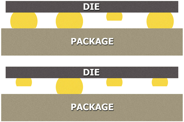
The term planarity, in flip-chip bonding, refers to the height consistency that exists across the top of all bumps. As shown (greatly exaggerated) in Figure 10, height variations can lead to uneven distribution of forces, die fractures and open circuits. Current requirements for planarity call for less than 5 µm of variation in bump height across the entire die.
Bump Shapes and How They Affect the Process
The optimization of any gold flip-chip process is achieved by optimizing the bump shape. The bump shown in Figure 11 is different from the typical bump in that it does not have the typical tail or pointy peak. New bump formation techniques have been developed that can create a gold bump without the traditional tail.
The bump seen here was designed specifically for a thermo-compression or a thermo-sonic bonding process. Note that there is a softer, more blunt peak to this bump. This shape will help direct the compression forces to assist in the formation of an inter-metallic bond at the second surface. By focusing the applied energy down to a smaller surface area, the other bonding factors (heat, force and ultrasonics) can be reduced. As this bump continues to be compressed, the surface area in contact will grow to increase the conductive path.
For the conductive epoxy solution, a shape like the one in Figure 12 may be preferred. This bump has a center stud and a matted finish around the top half. The finish was created by the impression of the capillary onto the gold ball. The capillary is the tool that carries the wire down to the surface to be bonded. It is the same tool that presses the gold ball onto the surface. This matted texture is favorable to the epoxy solution because it provides an optimized surface for conductive epoxy to adhere and remain in place during the flip and attach process.
The third shape discussed is the coined or flat-top shape. This is an attractive shape for the underfill process discussed earlier. Figure 13 shows a flat-top bump that looks similar to the coined shape. The flat top, in this case, was created using a shearing process across the top of the bump immediately after it was formed. Utilizing this process eliminates the need for a separate coining process.
Other Considerations
Underfill materials were usually necessary in the solder process but not always necessarily in the gold processes. Underfill materials add to the structural integrity of the completed die/bump package. An underfill material can help minimize the stresses occurring due to thermal coefficients of expansion differences between the die and the package. In other words, as the temperature changes, the die expands and contracts at a different rate than the package does. This can create stresses and strains in the connections. An underfill adds to the structural support of this completed package and will prevent some of the damaging stress that is associated with thermal cycling. Reduced stress will translate into better reliability in the long term.

Conclusion
Many manufacturers and packaging designers are looking for alternatives to the traditional solder flip-chip process. Gold bump solutions provide several advantages. There are a number of different gold bump processes that are available to meet the different bonding needs. Finally, the gold bump shape should be optimized to ensure the most efficient manufacturability and long-term reliability. Recent advances in bump technology allow the formation of flat-topped bumps without the added step of a coining process, providing a ready-made solution for packaging and process engineers.
References
1. K.J. Puttlitz, "Area Array Technology: The Basics and Packaging/Assembly Innovations," Die and Packaging-level Microelectronics Assembly: Base and Advanced Technology Course, San Diego, CA, November 2001. Available at www.dpla.org.
2. G. Riley, "Bump, Dip, Flip: Single Chip," Proceedings of 1997 Surface Mount International, September 1987, pp. 535-541.
Jerry Jordan earned his BS in mechanical engineering from the United States Naval Academy and his MBA from the Marshall School of Business at the University of Southern California. He has held several positions in manufacturing management for three companies, including the Xerox Corp., where he was selected to the "Operational Excellence" organization for his efforts in process improvement. Since joining Palomar Technologies in 2000, he has served as an applications engineer and a product marketing manager. He is currently focused on technical marketing to the broadband communications industry.