
Accurate, nonlinear, active device models are critical to achieving design success for circuits such as power amplifiers, oscillators and mixers, using computer-aided engineering (CAE) software such as Agilent Technologies' Advanced Design System (ADS™), Applied Wave Research's Microwave Office™, Eagleware's Genesys™ or Ansoft's Serenade™.
Prior work has made it clear that I-V measurements made under short (1 to 2 µs) pulse conditions can be helpful for transistor and diode modeling as well as semiconductor process improvement efforts.1-5 There are at least three issues that are addressed by pulsed I-V measurements, all of which cause a difference between the I-V characteristics affecting the clipping and nonlinear distortions of a large RF signal, as compared to the static I-V curves measured with a DC parameter analyzer or curve tracer. The three issues are trap or surface state occupancy, thermally induced changes in the output current due to self-heating of the device and the inability to perform measurements at DC power levels higher than those that can be tolerated continuously without destroying the device. This article reviews pulsed I-V basics and outlines a simple setup consisting of a commercially available dynamic I-V analyzer, a wafer probe fixture and a PC. To illustrate the importance of such measurements for transistor modeling, static and pulsed I-V measurements are compared for a PHEMT. Corresponding I-V fitting coefficients are extracted for three nonlinear models for the device. In order to illustrate a CAE application, one of the derived sets of fitting coefficients is used to exemplify I-V simulation with a nonlinear Angelov model6 setup within Microwave Office.
Background and Motivation for Pulsed I-V
Conventional nonlinear transistor and diode modeling utilizes a combination of static DC I-V measurements and S-parameter measurements made at multiple static bias conditions to extract the equivalent circuit element values. Extractions based on static biased measurements in many cases provide a good approximation to actual operation where the thermal and other "slow process" effects may be neglected. In other situations, the fact that the device temperature and deep level, or trap, effects can vary with each DC bias causes unacceptable errors between RF behavior and model predictions.
A deep level refers to an available energy level or site that can either give up an electron to the conduction band or accept an electron from the valence band. The terminology "deep" implies that the associated energy required to cause electron transfer is deep between, or removed from both, the valence and conduction band energy levels. As a consequence, the time scale associated with electron transfer through deep levels is much slower than those in normal microwave device operation due to intentionally introduced shallow acceptors or donors. Deep levels are sometimes referred to as traps, and traps can be associated with either surface states or defects and impurities in the bulk semiconductor. At suitably low frequencies (up to the kilohertz region), trap occupancy, and thus the charge distribution and channel depletion width in an FET channel, vary with bias condition and temperature. This causes dispersion in the I-V characteristics for diodes and transistors. For MESFETs and HEMTs, the dispersion is seen in the transconductance gm and output conductance gds, among other effects.
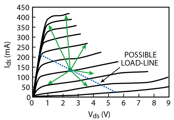
Whether or not trap effects are significant, the ability to make isothermal measurements is an advantage of pulsed I-V for any device where self-heating can be expected to affect the I-V behavior. Under normal RF operation, taking a class A amplifier for simplicity, the DC bias, and hence thermal condition and trap occupancy, remains unchanged as the RF signal swings along a load-line determined by the load impedance and the device parasitics. In general, the DC operating point can shift due to unequal clipping or distortion of a large RF signal (such as occurs in class AB and class B amplifiers). In contrast to the previously described device measurements made under varied static DC conditions, under RF operation, trap occupancy and thermal conditions are held essentially constant at values set by a single DC bias operating condition.
As demonstrated with several in-house research systems,1-4 pulsed I-V measurements can be setup to use a low duty cycle pulse of a duration such that both the traps and the device thermal condition are held at a quiescent DC bias point. The voltages are then pulsed and currents observed at different instantaneous points at rates that approximate those present under large signal RF voltage swings. One solution to the problem, available commercially from Agilent Technologies, allows for performing both current and S-parameter measurements under fast-pulse conditions.7,8 This system combines a DC parameter analyzer, a pulse generator, RF synthesizers, a digital scope and a pulsed network analyzer, along with other instruments controlled by external software. Such a pulsed RF/pulsed DC test system has been shown to be effective in challenging modeling problems such as LDMOS power transistors capable of very high RF power, with high DC bias and thermal dissipation requirements.9 A similar pulsed I-V/pulsed RF research system was developed at Texas Instruments prior to this.10 In one study, the TI system was used to show that trap effects cause a notable shift in both I-V and C-V characteristics for a GaAs Schottky diode.11 Another commercial solution is the Dynamic I-V Analyzer (DIVA), originally developed by GaAsCode Ltd., and recently redesigned by Accent Optical Technologies.12-14

Pulsed I-V Measurement Basics
The diagrams shown in Figures 1 and 2 illustrate the pulsed I-V measurement process for the case of a MESFET or HEMT. A fast pulse with a low duty cycle is used to move the gate and drain biases from a chosen steady quiescent bias to another point on the I-V plane. The idea is that the pulse width  , typically on the order of microseconds or less, is much shorter than the time, on the order of milliseconds or longer, required for either the trap occupancy or the device thermal condition to change. The thermal condition is set by the quiescent bias condition according to
PDiss = VdsQ x IdsQ (1)
where VdsQ and IdsQ are the quiescent drain voltage and current. For a given device there is a maximum power dissipation for safe operation, beyond which the device stands a good chance of being destroyed. Maximum conditions for power dissipation and/or drain current and voltage are typically included in the device specification sheet.
The actual device channel temperature will depend on the heat sink temperature and the thermal resistance of the device. The relationship between steady-state device operating temperature Top and ambient heat sink temperature Tamb is given by
Top = ( TH x Pdiss) + Tamb (2)
where
TH = thermal impedance between the device and the heat sink
The period of the pulse train tr is set to be greater than the thermal time constant to maintain the quiescent thermal condition established by Equation 1, while pulsing to other bias conditions instantaneously.
Instrumentation and Measurement Setup
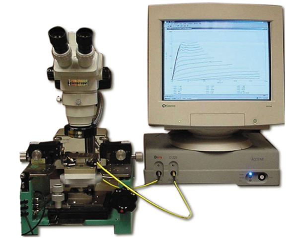
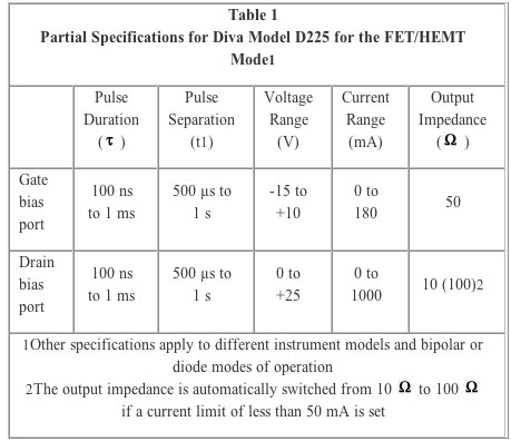
Figure 3 shows a basic pulsed I-V setup consisting of an Accent model D225 dynamic I-V analyzer (or DIVA) instrument connected to a J microTechnology Personal Probe Station™. The system is run from a standard PC running Microsoft Windows 2000 using the DIVA operating software. For probe station use, DC needle probes are not acceptable due to the inductive loading they create on the pulsed measurement. Instead microwave ground-signal-ground probes (GGB Industries 40A-GSG-150-P) are used to make on-wafer device connections. A set of partial specifications for the D225 is shown in Table 1.15
The software has a graphical user interface through which the user sets up various parameters of the measurement. Inputs for FET/HEMT measurements include the minimum and maximum values for static or instantaneous voltages (minimum Vds is always zero, Vgs can range from negative to positive), the maximum static or instantaneous drain current and the maximum instantaneous power dissipation allowed. Setup information for static I-V measurements includes the number of samples to be averaged for each I-V data point, the Vgs step size and the sweep rate. For pulsed measurements, the user specifies additionally the nominal steady quiescent bias point and, in place of the sweep rate specified for static measurements, the Vds step size, the pulse length () and the pulse separation (r).
Stability and ringing are two practical considerations arising in pulsed measurement. To avoid instabilities, parasitics in the fixturing and connections need to be minimized and, in some cases, specific external device stabilization networks may be required. Still, undesired oscillation can occur in high gain devices even under resistive loading presented by the configuration of the measurement setup. Long cables cause reactive loading of the pulsed measurement, which can decrease device stability or cause ringing in the pulse waveform. Hence, as a general practice, cable length should be kept to a minimum.
Example Measurements

The previously described setup was used to measure the static and pulsed I-V characteristics of a 600 µm PHEMT to explore the advantages of dynamic I-V measurements. The data for both sets is shown in Figure 4. For the pulsed measurements, the quiescent voltage and current conditions were 2.5 V and 135 mA, respectively. The limits imposed on the device were Vds = 9 V and Ids = 420 mA. The pulse duration was set at 0.2 µs with a pulse separation of 1 ms. The differences between pulsed and static measurements are seen, especially for the higher drain currents. This is consistent with the higher power dissipation, and correspondingly greater temperature differences (between the static and pulsed measurement conditions) at larger values of voltage and current, according to Equation 1. There is a notable difference in the slope of the Ids versus Vds curve, that, for currents below 200 mA, corresponds to the well-known dispersion in gds (=  Ids/ Vds).16 At higher currents, this slope becomes negative for the static measurements, an effect often attributed to thermally-induced current reduction. From previous modeling efforts, the pulsed data represents better the RF gds as well as the transconductance, gm (= Ids/Vgs).5,8
Figure 5 shows the results of a pulsed measurement of the breakdown voltage for the same device. A pulsed breakdown measurement has less chance of destroying the device, and produces a breakdown characteristic that is likely to be more representative of that seen under large signal RF conditions. A few attempts to pulse to higher currents for this breakdown measurement caused failure for the selected PHEMTs.
Curve Fits for Nonlinear Models
Model parameters for Statz,17 TOM18 and Angelov6 nonlinear models were extracted separately for pulsed and static data sets. Table 2 compares the resulting fitting coefficients, which show notable differences between the static and pulsed I-V cases. These coefficients are initial model results achieved through an extraction routine available in the DIVA software.
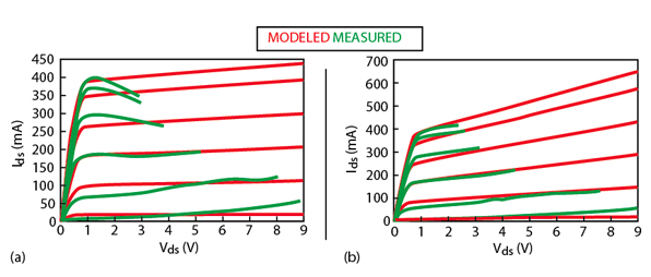
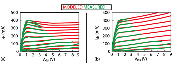
Figures 6, 7 and 8 show various nonlinear model curve fits compared to the static and pulsed data sets, respectively. The simulated curves were generated in ADS and Microwave Office by inputting the parameters from Table 2 into the Statz, TOM and Angelov models built into the simulators. Several observations can be made. The three models are notably different in their abilities to fit various regions of the I-V curve sets. For the static data, the TOM model has the ability to fit the negative slope region of the I-V curves in the high current region, while the Statz model does a better job in the low current/low voltage region. For this particular device, the Angelov model provides the best overall curve fit.
To take the exploration one step further, the Angelov dynamic I-V model was used in the AWR Microwave Office and modified to model the breakdown effect seen. Figures 9 and 10 show the Microwave Office setup and results. The current fitting coefficients of Table 2 are entered directly. The simulations were extended past the breakdown voltage to illustrate the entire I-V region that a large RF signal may experience in a dynamic sense. Note that in the TOM and Statz models, the breakdown (not shown) is typically specified in the simulation setup as a single parameter and the breakdown model has a much sharper characteristic than seen in the pulsed breakdown measurement. The Angelov model has additional parameters that allow for modeling the soft breakdown characteristic observed from the pulsed I-V measurement.

|
Table 2 | ||
|
TOM Model Coefficients | ||
|
Parameter |
Static |
Dynamic |
|
Alpha |
2.320 |
2.656 |
|
Beta |
0.2697 |
0.2473 |
|
Delta |
1.4e - 18 |
0.0836 |
|
GammaDC |
0.034 |
0.0343 |
|
Q |
0.833 |
0.833 |
|
Vto |
-0.996 |
-0.810 |
|
Statz Model Coefficients | ||
|
Parameter |
Static |
Dynamic |
|
Alpha |
3.032 |
3.498 |
|
Beta |
7.913 |
1.603 |
|
Lambda |
0.0162 |
0.0970 |
|
Theta |
36.900 |
7.587 |
|
Vto |
-1.105 |
-1.105 |
|
Angelov Model Coefficients | ||
|
Parameter |
Static |
Dynamic |
|
Ipk |
206.24 |
193.70 |
|
P1 |
0.8299 |
1.0210 |
|
P2 |
-0.2741 |
-0.1338 |
|
P3 |
0.3291 |
0.3829 |
|
B1 |
0.9787 |
0.4345 |
|
B2 |
0.3506 |
0.02474 |
|
Vpks |
-10.1157 |
-1.3610 |
|
Vpk0 |
-0.5633 |
-0.6364 |
|
AlphaR |
0.5325 |
0.2173 |
|
AlphaS |
0.8471 |
0.9693 |
|
Lambda |
0.0147 |
-0.0665 |

Conclusion
Pulsed I-V measurements provide a means to more properly address dispersion and thermal effects in microwave devices, as compared to conventional static I-V measurements. Recent advances in commercial instrumentation allow these measurements to be made with setups quite simple compared to various research setups described in the literature. The presented setup can be used to obtain pulsed I-V measurements for nonlinear device modeling or device evaluation/improvement purposes. In the example given, a set of dynamic I-V curves for a 600 µm PHEMT device were shown to provide the basis for implementing a nonlinear model for the device. A multitude of nonlinear models are available for transistor modeling, and one of the key differences is in the equations used to fit the I-V curves. The best model choice depends on the device and its dynamic I-V behavior, as there is, to date, no "one model fits all" solution. Efficient extraction of dynamic I-V models allows the device modeler to concentrate on the remaining tasks of fitting the device charge, or capacitance functions, and its parasitic elements using S-parameter data to complete the modeling process.

Acknowledgment
The authors would like to thank James Bridge of Accent Optical for his helpful editing suggestions.
References
1. M. Paggi, P. Williams and J. Borrego, "Nonlinear GaAs MESFET Modeling Using Pulsed Gate Measurements," IEEE Transactions on Microwave Theory & Techniques , Vol. 36, No. 12, December 1988, pp. 1593-1597.
2. J. Vidalou, F. Grossier, M. Camiade and J. Obregon, "On-wafer Large Signal Pulsed Measurements," 1989 IEEE MTT-Symposium Digest , pp. 831-834.
3. A. Platzker, A. Palevsky, S. Nash, W. Struble and Y. Tajima, "Characterization of GaAs Devices by a Versatile Pulsed I-V Measurement System," 1990 IEEE MTT-Symposium Digest , pp. 1137-1140.
4. E.L. Nelson, "Pulsed I-V Test Set," University of South Florida, 1990.
5. P. Ladbrooke and J. Bridge, "The Importance of the Current-voltage Characteristics of FETs, HEMTs and Bipolar Transistors in Contemporary Design," Microwave Journal , Vol. 45, No. 3, March 2002.
6. I. Angelov, H. Zirath and N. Rorsman, "A New Empirical Nonlinear Model for HEMT and MESFET Devices," IEEE Transactions on Microwave Theory & Techniques , Vol. 40, No. 12, December 1992.
7. M. Dunn and B. Schaefer, "Link Measurements to Nonlinear Bipolar Device Modeling," Microwaves & RF , February 1996, pp. 114-130.
8. J. Scott, M. Sayed, P. Schmitz and A. Parker, "Pulsed Bias/Pulsed RF Device Measurement System Requirements," European Microwave Conference, 1994, Cannes, France, pp. 951-961.
9. J. Pla, Personal Communication, Motorola SPS, Tempe, AZ, June 2001.
10. S. Pritchett, Personal Communication, Texas Instruments, Dallas, TX, September 1990.
11. P.B. Winson, "Characterization and Modeling of GaAs Schottky Barrier Diodes Using an Integrated Pulsed I-V/Pulsed S-Parameter Test Set," University of South Florida, May 1992.
12. GaAs Code Ltd., "A Pulsed-measurement Instrument for Device Testing," Microwave Journal , Vol. 42, No. 6, June 1999, p. 122.
13. P.H. Ladbrooke, N.J. Goodship, J.P. Bridge and D.J. Battison, "Dynamic I-V Measurement of Contemporary Semiconductor Devices," Microwave Engineering Europe , May 2000.
14. P.H. Ladbrooke, J.P. Bridge, N.J. Goodship and D.J. Battison, "Improving Understanding of the RF Circuit Behaviour of Contemporary Semiconductor Devices Through Fast-sampling I-V Curve Tracer Measurements," GaAs 2000 Conference, Session G15, Paris, France, October 2000.
15. Accent DIVA Models D210, D225, D225HBT, D265 Dynamic I-V Analyzer, User Manual, Issue 1.0 (P/N 9DIVA-UM01), 2001, Accent Optical Technologies, Bend, OR.
16. C. Camacho-Penalosa and C.Aitchison, "Modeling Frequency Dependence of Output Impedance of a Microwave MESFET at Low Frequencies," i , Vol. 21, June 1985, pp. 528-529.
17. H. Statz, P. Newmann, W. Smith, R. Pucel and H. Haus, "GaAs FET Device and Circuit Simulations in SPICE," IEEE Transactions on Electron Devices , Vol. ED-34, No. 2, February 1987.
18. A. McCamant, G. McCormack and D. Smith, "An Improved GaAs MESFET Model for SPICE," IEEE Transactions on Microwave Theory & Techniques , Vol. MTT-38, No. 6, January 1990.