
Frequency synthesizers are used in a variety of communications and timing systems. Phase-locked loops (PLL) have been the "workhorse" of the majority of traditional synthesizers and clock generation circuits. However, there are other types of synthesis blocks available such as direct digital synthesizers (DDS), mixers, frequency doublers and dividers that can be used to create frequency synthesis systems with enhanced performance characteristics. Often these other synthesis blocks can be used in combination with standard PLL techniques in what are sometimes referred to as hybrid synthesis loops.
Understanding the basic attributes of the various synthesis blocks will aid in determining how they may best be combined in order to achieve the desired performance. The primary figures of merit for frequency synthesizers are spurious response and noise performance, frequency tuning resolution, frequency switching time and low power.
To begin, the individual characteristics of several types of synthesis blocks will be explored, followed by a demonstration of how these blocks can be combined to form various types of hybrid synthesizers. Bench data for many of the synthesizers discussed will be presented.
Phase-locked Loop
As basic PLL characteristics are considered from a functional point of view, emphasis will be provided on the loop attributes affecting spurious responses (spurs), noise and switching speed. In frequency synthesizer systems, PLLs are most commonly used as frequency multipliers. The ratio of the frequency at the PLL output to the input reference frequency is set by the divider ratio N. In effect, a PLL acts as a tracking bandpass filter with the filter bandwidth being determined by the closed loop transfer function. A PLL block diagram and the closed loop transfer characteristic for a basic, second-order, type II PLL are shown in Figure 1 and Equation 1.

where
s = generalized frequency variable in Laplace transform
 n = natural frequency of the PLL loop
 = loop damping ratio
(See References 1 and 2 for discussion of PLL order and type designation.)
As shown in the closed loop transfer characteristic, the PLL input phase noise (or spurs) is increased by a factor of 20 log N within the loop bandwidth. Outside the loop bandwidth, the phase response is attenuated at a rate of -20 dB per decade. In practice, higher order poles are usually added to the loop filter in order to achieve additional attenuation.
Another key PLL characteristic is that the phase noise (PN) contribution of the voltage-controlled oscillator (VCO) is attenuated by the loop at frequencies within the loop bandwidth. At frequencies outside the loop bandwidth, the VCO phase noise directly contributes to the loop phase noise. Therefore, loops with wider bandwidths attenuate the VCO noise over a wider bandwidth. Equation 2 and Figure 2 show the VCO noise rejection transfer function for a second-order, type II loop. The slope of the VCO noise attenuation curve within the loop bandwidth is 40 dB per decade.

In a traditional integer-N PLL, the tuning resolution is limited by the input reference frequency. Since tuning is achieved by adjusting the divider value, restricting the divider or prescaler to integer values limits the resolution available at the output. This constraint on the input frequency also has implications for switching speed as the loop bandwidth must be set to a factor of 1/10 or less than the input reference frequency to provide for loop stability.
In PLL analysis, the loop is often approximated by a linear control system model. The previously displayed frequency response equations show this approach. Laplace transforms allow time domain or transient properties such as settling time to be evaluated in a similar manner. A good assumption for a linearly approximated loop is that the settling process occurs within one cycle of the loop resonant frequency:

where
Ts = settling time
Notice the inverse proportionality of the settling time to the loop's natural frequency, as well as to the loop bandwidth; the two are related as

This highlights one of the key tradeoffs in PLL system design: designing the loop for a wider loop bandwidth can decrease settling time, but reduces its ability to filter input phase noise.
At the next level of analysis of PLL transient characteristics, the loop cannot always be treated as a linear model for all magnitudes of frequency excursion. The frequency range over which a loop can be considered as closely approximating linear switching performance is usually defined as the lock range . Beyond the lock range, an event referred to as cycle slipping starts to occur. Within the range that cycle slipping occurs, the phase detector and charge pump are charging up the capacitance in the loop filter at a maximum rate that is primarily dependent on the phase detector architecture and the magnitude of charge pump current. The time for a loop to switch from a frequency outside the lock range to within the lock range is the pull-in time. For a given loop configuration, the pull-in time , as well as the lock time, can be estimated with reasonable accuracy, whereas simulations provide excellent accuracy. The overall frequency switching time is the combination of the pull-in time and the lock time (Best1 provides an excellent treatment of transient characteristics of PLLs).
Fractional-N PLLs are currently becoming available, which overcome many of the obstacles associated with integer-N PLLs. Fractional-N PLLs effectively achieve fractional division ratios which provide finer frequency tuning resolution while using higher input reference frequencies. This allows wider loop bandwidths, and enables faster switching times and better VCO noise attenuation. The resolution of a fractional-N PLL can be quite fine, with fractional ratios on the order of 1:224. Practical loop bandwidths are still somewhat limited because the process of generating the fractional division can create spurs that must be filtered, or attenuated by the loop. The predominant architecture for fractional-N PLLs is the delta sigma (
 ) approach that shapes the in-band noise and places much of it outside the loop bandwidth.
Dividers and Squaring Circuits
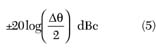
The divider function has an interesting characteristic: phase noise and spurs at the divider input are attenuated by the division process. The level of attenuation is -20log N. This is useful in synthesis applications beyond the PLL. One way of understanding this is to view the phase noise at a divider input as narrow band phase modulation. The spurs for narrow band phase modulation are equal to
where
 = phase error associated with the level of phase noise or spurs
Just as frequency can be equated to the reciprocal of period in the time domain, can also be related to jitter, or time-base error. Dividing the input frequency by two increases the period by a factor of two while the jitter or time error is unchanged. This assumes that the added jitter from the divider itself is negligible. If the jitter is unchanged and the period is increased by a factor of two, the phase error relative to 2  (one complete cycle) is also decreased by two. This results in the 6 dB per octave attenuation property of a divider. This characteristic is demonstrated by the bench measurements shown in Figure 3 where a divide-by-eight circuit attenuates the spurs on the input signal by approximately 18 dB at the divider output. The plot also shows that the "noise skirt" around the fundamental is attenuated.
It is important to recognize the limitation of this ability to attenuate PN and spurs. The divider logic will have its own phase noise floor (or jitter performance) that will set the limit on the actual PN performance achievable at the divider output. Also, if the divider is followed by a buffer or amplifier, the additional PN of these blocks needs to be considered because they can significantly raise the total PN of the system.
The inputs of divider circuits often contain a squaring (or limiter ) function. Limiters are used in synthesis applications where it is necessary to convert sinusoidal signals to logic level signals for processing by digital blocks, such as dividers or phase detectors. The frequency domain characteristics of the limiter function must be considered. A limiter converts amplitude modulation (AM) spurs into phase modulation (PM) spurs. A conversion constant with units of degrees/decibel can be determined by measurement of the limiting stage. This conversion constant depends upon the input signal power, internal gain and slew rate of the stage. It is a measure of delay versus instantaneous input signal. If an input signal to an ideal limiter consists of a carrier and a single sideband spur that modulates the threshold of the limiter, then a phase error dependent on the conversion constant is produced at the output. This phase error can be treated as narrow band phase modulation with the resultant splitting of the spur into two sidebands, along with a 6 dB attenuation of the spur. Bench measurement of this process is shown in Figure 4 where the large single-sided spur is converted to double sideband spurs with approximately 6 dB of attenuation (Manassewitsch3 contains a rigorous treatment of the frequency characteristics of limiting circuits).
It is interesting to note that since the output of the ideal limiter is a square wave, the images of the spurs are present around the odd harmonics of the fundamental frequency. In this respect, the ideal limiter acts like a mixer.
Alternative Synthesis Blocks
Mixers
Mixers are often used in synthesizers to achieve frequency translation. Note the term translation as opposed to multiplication ; both up- and down-conversion modes are used.
Synthesizers that use a mixer to up-convert a lower frequency tunable reference to the low or high side of the fixed local oscillator (LO) are sometimes referred to as direct synthesizers . In some cases, mixers can be used in the feedback loop of a PLL in either up- or down-conversion modes of operation.
A mixer combines two inputs to create an output. One of these is the LO, the other is either the RF, or IF, depending on whether the mixer is used for up- or down-conversion. The LO acts as an ideal switching signal (square wave) for the other input. The LO is fixed in frequency, whereas the IF, or RF, is tunable. An ideal mixer would simply translate an input signal (RF or IF) to a new frequency without providing any gain to spurs or PN. The equation for an ideal fully balanced mixer response is

The spectral content is shown in Figure 5 . As can be seen, images of the desired signal are generated around the odd harmonics of the LO frequency (since the LO is a square wave). Usually only the high or low side of the first image is desired, so the unwanted images must be filtered out.
Mixers are characterized by their nonideal intermodulation products. These are very important in receiver applications. In some synthesizer applications, frequency planning can place intermodulation products out of band so that the most important mixer attribute may be its noise floor or PN, a parameter rarely seen on mixer data sheets.
In hybrid synthesizers utilizing mixers, an additional frequency reference must be provided to act as the LO. The performance benefits of this technique must be balanced with the added complexity and cost of this LO source.
Direct Digital Synthesizers
Direct digital synthesis circuits are finding increased use in synthesizers as well as in digital modulators and demodulators. DDS is almost a purely digital means of generating a signal that, for synthesizer applications, is most commonly a sinusoidal waveform. The DDS core creates a digital representation of the sine wave, which is then converted into the analog domain. A block diagram of a DDS is shown in Figure 6 . A basic DDS consists of an accumulator that accepts a frequency tuning word, a phase-to-amplitude converter and a digital-to-analog converter (DAC). The width (in bits) of the tuning word defines the resolution, or frequency granularity, of the synthesizer. The output of the accumulator is the numerical phase of the generated signal.
The accumulator is typically truncated to a bit-width that is a few bits wider than the DAC bit-width. The extra bits insure that the phase errors do not degrade the spectral quality of the signal more than does the DAC quantization error. The amount of truncation has implications for the spurious performance of the DDS. The bits that are truncated in effect act as a digital phase noise generator that modulates the carrier signal. The maximum level of the truncation spurious is determined by the bit-width of the non-truncated bits, and is approximately
-6.02P dBc (7)
where
P = bit-width going into the phase-to-amplitude conversion block
There are special cases where the worst-case spur deviates from this, but the above relationship is true for most practical tuning word values.
The phase-to-amplitude block can be imagined as a read-only memory (ROM) look-up table. The ROM output values correspond to the closest amplitude point available for a given phase value (the input). This process of rounding to the nearest DAC code generates an amplitude error for each phase point that produces the amplitude quantization noise floor. The spurs created by this process are sometimes referred to as AM spurs. A good approximation for the peak AM spurs for most practical tuning words is
-6D -12 dBc (8)
where
D = DAC bit width
The signal-to-noise ratio for a DDS system is given by
-1.76 + 6.02D (9)
In practice, most implementations of the phase-to-amplitude block do not use a pure ROM table approach. There are a variety of techniques to reduce the hardware required to perform the conversion. The most efficient techniques use digital signal processing algorithms that perform a real time computation of the amplitude. Various implementations trade spurious performance for circuit efficiency, but the basic goal is that the spurs generated by the algorithm should approximate the spurious performance achievable with the ROM approach.
Note that the quality of the DAC can be the limiting factor in the synthesizer's spectral performance. DAC nonlinearity and nonideal transient performance can cause many of the worst spurs. Sophisticated DDS users are aware of these DAC generated spurs and often use frequency planning to place them out of the band of interest.
The output frequency of a DDS is determined by
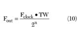
where
W = bit-width of the tuning word, going into the phase accumulator
TW = tuning word value
The resolution is therefore set by Fclock/2n. In commercially available DDSs, the tuning word ranges from 32 to 48 bits. DDSs therefore provide the finest tuning resolution of any of the synthesizer forms. DDS has other advantages as well. Note that the DDS resembles a very fine resolution clock divider. The phase noise on the clock of a DDS is attenuated in a similar fashion as in the divider block described earlier. Also, since the DDS is an open loop, purely digital system, it exhibits extremely fast frequency switching performance. The transition from a given frequency to another takes place within one system clock cycle, and in a phase continuous manner. There is a deterministic fixed latency from the time a frequency change is "registered" until it becomes active on the DAC output.
Compared to other forms of synthesis, DDSs have unmatched frequency switching speed and tuning resolution. They exhibit extremely good phase noise performance. It is increasingly inaccurate to perceive a DDS as limited by its spurious performance and excessive power consumption. In fact, DDSs with 14- to 16-bit output resolution clock rates as high as 400 Msps, and power less than 250 mW are imminent (see Reference 4 for an in-depth tutorial on DDS technology and current products).
Doublers and Triplers
Doublers and triplers provide low integer ratios of frequency multiplication with relatively high levels of performance. As with all frequency multiplication blocks, the spurs and phase noise are increased by 20 log N. They can be simpler to use than mixers in that they do not generate the large number of spurious signals due to intermodulation products. These blocks are not typically loop based and therefore do not have the frequency switching limitations of PLLs. They may, however, contain band-limiting filtering at their inputs, and/or outputs, in order to suppress unwanted spectral components. These blocks are useful when the fine-tuning is provided by a DDS or PLL loop, but the maximum frequency output of either of these circuits is too low. This can be a real benefit for a DDS where the maximum output frequency is constrained by the maximum switching speed of the digital circuitry (in CMOS implementations of DDS, the power dissipation is proportional to the system clock rate). An efficient doubling circuit at the output of a DDS will increase the bandwidth of the DDS circuit by a factor of two without the power penalty incurred by running the entire DDS system at twice the clock rate. Similarly, in a PLL system where the VCO maximum frequency is limited, a doubling circuit can extend the bandwidth of the synthesizer.
There can be a significant amount of conversion loss in passive doublers. Often active amplifiers are used with doublers to provide power gain. There are several methods of designing doublers or higher order multiplying circuits. Some are based on generating harmonically rich signals and filtering the output to extract the desired signal. One type of doubling circuit that provides very good wide band performance is shown in Figure 7 . This rectifier-based circuit can be implemented with transformers or baluns. The ripple frequency that is inherently generated in this type of circuit provides the doubling mechanism. Conversion losses of 10 to 15 dB are typical in this type of doubler (see Reference 5). Another method of achieving an odd-order multiplier is to feed a filtered DDS output signal into a limiting circuit and then use a bandpass filter to select the desired odd harmonic.
Hybrid Synthesizers
One simple hybrid synthesizer topology consists of a DDS circuit driving a divider, as shown in Figure 8 . As mentioned earlier, the divider circuit will attenuate the phase noise and spurs of the DDS by 20 log N.
A disadvantage of this arrangement is that the synthesizer's frequency range is reduced. If a DDS with sufficiently high frequency capability is used, the division process improves the phase noise and spurious response, while sacrificing bandwidth. A hybrid synthesizer that maintains bandwidth but adds some complexity includes a mixer block. The mixer requires a fixed LO signal. This circuit is shown in Figure 9 .
The DDS drives the IF input of the mixer, while the mixer is used to up-convert the signal around the LO. The signal can then be filtered to attenuate the unwanted image. The signal is then processed by the divider to a lower frequency. This lower frequency could simply be the original DDS output frequency. The aim of this synthesizer is to up-convert the signal with negligible degradation of spurious and phase noise performance, and then realize spurious and phase noise improvements because of the division process. In an actual system, the mixer and divider will have their own noise floor limitations that will impact the actual performance. Bench measurements of the spectra for the various points in this synthesizer are shown in Figure 10 . Multiple "mix-and-divide" blocks can often be cascaded in order to attenuate the spurs to very low levels.
Another simple configuration to double the bandwidth to a DDS based synthesizer is shown in Figure 11 . It consists of a DDS followed by a comparator limiting circuit that drives a passive doubler. Figure 12 shows the operation of this circuit.
The limiter effectively increases the level of the DDS output signal in order to drive the doubler at a higher power level. This compensates somewhat for the doubler's conversion loss. The spurs are attenuated by approximately 6 dB by the limiter and then increased by 6 dB by the doubler so that the maximum spurious free dynamic range at the output is approximately the same as at the input. Another method of frequency doubling is through the use of a quadrature DDS and a mixer, as shown in Figure 13 .
A quadrature DDS contains two DAC outputs that generate sinusoidal signals in quadrature (offset in phase by 90°). One of the outputs drives the LO port while the other output drives the IF port. One mixer image occurs at DC, with the other at twice the DDS output frequency.
Even DDSs that do not provide quadrature outputs usually have a phase register that allows the phase to be adjusted. Two DDSs can be adjusted to quadrature by means of this phase adjustment (a means to synchronize the two DDSs is usually provided).
Another hybrid synthesizer consists of the DDS driving a PLL, as shown in Figure 14 . This circuit exhibits the excellent frequency resolution of the DDS, while the PLL provides the up-conversion to higher frequencies as well as the filtering benefits of a band-limited system. With this circuit, the spurs and phase noise levels of the DDS are increased within the loop bandwidth of the PLL. Bench measurements are given in Figure 15 where the multiplication value is 16, and the spurs and noise increases are clearly shown. The dominant spur is observed to have grown by about 19 dB. Approximately 24 dB of growth might be expected, since the loop divider value is 16. This apparent discrepancy can be explained - the DDS output is a sine wave with a dominant spur. The input to the PLL phase detector contains a squaring circuit. As discussed previously, the squaring circuit will convert the dominant spur into two spurious sidebands with 6 dB of attenuation. Relative to this level, 24 dB of gain should then be expected. The net growth of peak spurs relative to the carrier should then be about 18 dB. It has been observed that if there are multiple, closely spaced, relatively low level spurs at the squaring circuit input, the 6 dB attenuation cannot necessarily be relied upon. This is due to the sensitivity and speed of the squaring input and the effect of the arbitrary phases of the multiple tones.
A worst-case spurious condition is used in this example in order to clearly demonstrate the loop gain principles. In practice, frequency planning can be used in DDS configurations to provide spurious performance more like that shown in Figure 16 . The clock frequency of the DDS is altered to change the fclock/fout ratio such that the output frequency is the same as before, but placed in a spectrally purer region.
A simpler variant of this design puts the DDS in the feedback loop, as shown in Figure 17 . The VCO output can drive the DDS clock input directly if the DDS clock input circuitry has adequate bandwidth.
Some DDS circuits are now available with high frequency dividers on the clock input that enable higher frequency loops. One advantage of this configuration is that the cost, space and noise of the divider that the DDS replaces are removed. This circuit, however, shares the same limitation as the one using a DDS driving a PLL - the DDS phase noise and spurs are increased within the loop bandwidth.
One hybrid synthesizer that removes this performance issue is the offset or translation loop shown in Figure 18 . This synthesizer uses a DDS and a PLL loop in conjunction with a mixer to realize a loop with excellent spurious and noise performance, although with some added complexity.
The DDS creates a tunable reference frequency for the loop. The PLL loop provides a tracking bandpass filter. The mixer in the feedback loop down-converts the synthesizer output to the frequency range of the phase detector input. Since the feedback loop consists of frequency translation, not division, the gain in the loop is unity. This means that the spurs and phase noise of the DAC are not increased within the loop bandwidth. This allows wider loop bandwidths that enable faster frequency switching capability while maintaining good spurious and noise performance. Figure 19 shows bench data for this loop. The input for this circuit is the signal shown for a synthesizer with an alternate frequency plan. As can be observed there is no appreciable gain in the spurious noise floor, and the signal is effectively translated up to RF. These types of synthesis loops are often referred to as dual loop solutions because the mixer reference is usually generated by a fixed frequency PLL loop. The phase noise of the fixed loop that feeds the LO port of the mixer is filtered by the main loop. Integrated circuits with DDS, PLL and mixer circuitry all on the same chip are beginning to appear. Figure 20 shows a related configuration.
Note that in this configuration the DDS output is up-converted directly by the loop output frequency. The DDS spurs and noise levels are not increased within the loop bandwidth since the input to the divider is just the offset DDS signal.
Figure 21 shows a high performance hybrid loop that uses a mix-and-divide stage to attenuate DDS spurs. A translation loop generates a very high quality signal at the output. It should be pointed out that the mixer in the mix-and-divide stage will generate intermodulation products that could fall within the band of interest. Frequency planning with respect to LO1 and LO2 may be required to find an area of operation free of DDS spurs and mixer intermodulation products.
In order to demonstrate how noise is processed through this loop the worst-case input signal used in the synthesizer using a DDS driving a PLL is fed into this loop. Figure 22 shows that the signal is up-converted to the same RF as before, with the spurs actually attenuated by approximately 16 dB. This loop provides spur attenuation within the loop bandwidth thus enabling wide loop bandwidths and fast switching.
Conclusion
The preceding circuits demonstrate some, but by no means all, of the types of hybrid synthesizer circuits that can be designed. Each application requires a balancing act between cost, power, switching speed, frequency range and required spectral performance. Understanding the attributes of the different types of synthesis blocks available allows a wider range of possible solutions.
References
1. R.E. Best, Phase-locked Loops Theory, Design and Applications , Second Edition, McGraw Hill, 1993.
2. P.V. Brennan, Phase-locked Loops: Principles and Practice , McGraw Hill, 1996.
3. V. Manassewitsch, Frequency Synthesizers Theory and Design , Third Edition, Wiley Interscience, 1987.
4. Data converters, DDS tutorial, application notes and DDS product data sheets, www.analog.com.
5. Technical library, application notes on multipliers and other synthesizer topics, www.wenzel.com.
David Crook is a design engineer and product line manager for the high speed converter group of Analog Devices in Greensboro, NC. He has been with the company for fifteen years, and has most recently been involved with the development of BiCMOS and CMOS DDS-based synthesizer architectures.
 block diagram and (b) type II, second order closed loop transfer characteristic.")

 before division by eight and (b) after division.")
 input signal with single-sided spur and (b) output after processing.")


.")
 DDS output, (b) mixer output and (c) divider output.")

 DDS output, (b) limiter output and (c) doubler output.")


 input of f<sub>0</sub> = 100 MHz and (b) output of 16 f<sub>0</sub> = 1.6 GHz.")
 input and (b) output.")


